Assemblies having stacked semiconductor chips and methods of making same

Inactive Publication Date: 2006-07-04
TESSERA INC
View PDF135 Cites 121 Cited by
  • Summary
  • Abstract
  • Description
  • Claims
  • Application Information

AI Technical Summary

Benefits of technology

[0013]In another preferred embodiment of this present aspect of the invention, the microelectronic elements comprise semiconductor chips. A core panel chip is mounted to the core panel and connected to terminals disposed on the core panel and to traces extending to the side panels. Chips mounted on the side panels are connected to the core panel chip through the traces. Preferably, the terminals on the core panel are movable with respect to the core panel chip to relieve mechanical stresses caused by differential thermal expansion of the circuit board and chips during bonding and operation of the stacked assembly. In certain applications of this embodiment of the invention, the core panel is a processor chip, and side panel chips are memory chips. In other embodiments of the invention, one of the side panels is disposed at the top or bottom of the stack rather than having the core panel disposed in such a position, with terminals disposed on the side panel and exposed for connection to an external circuit.
[0014]Another aspect of the invention can increase the yield of stacked chip assemblies during manufacture. In particular, while portable devices may have differing processor and memory requirements—

Problems solved by technology

In particular, while portable devices may have differing processor and memory requirements—these requirements may overlap or be subsets of one anoth

Method used


Image

  • Assemblies having stacked semiconductor chips and methods of making same
  • Assemblies having stacked semiconductor chips and methods of making same
  • Assemblies having stacked semiconductor chips and methods of making same

Examples


Example

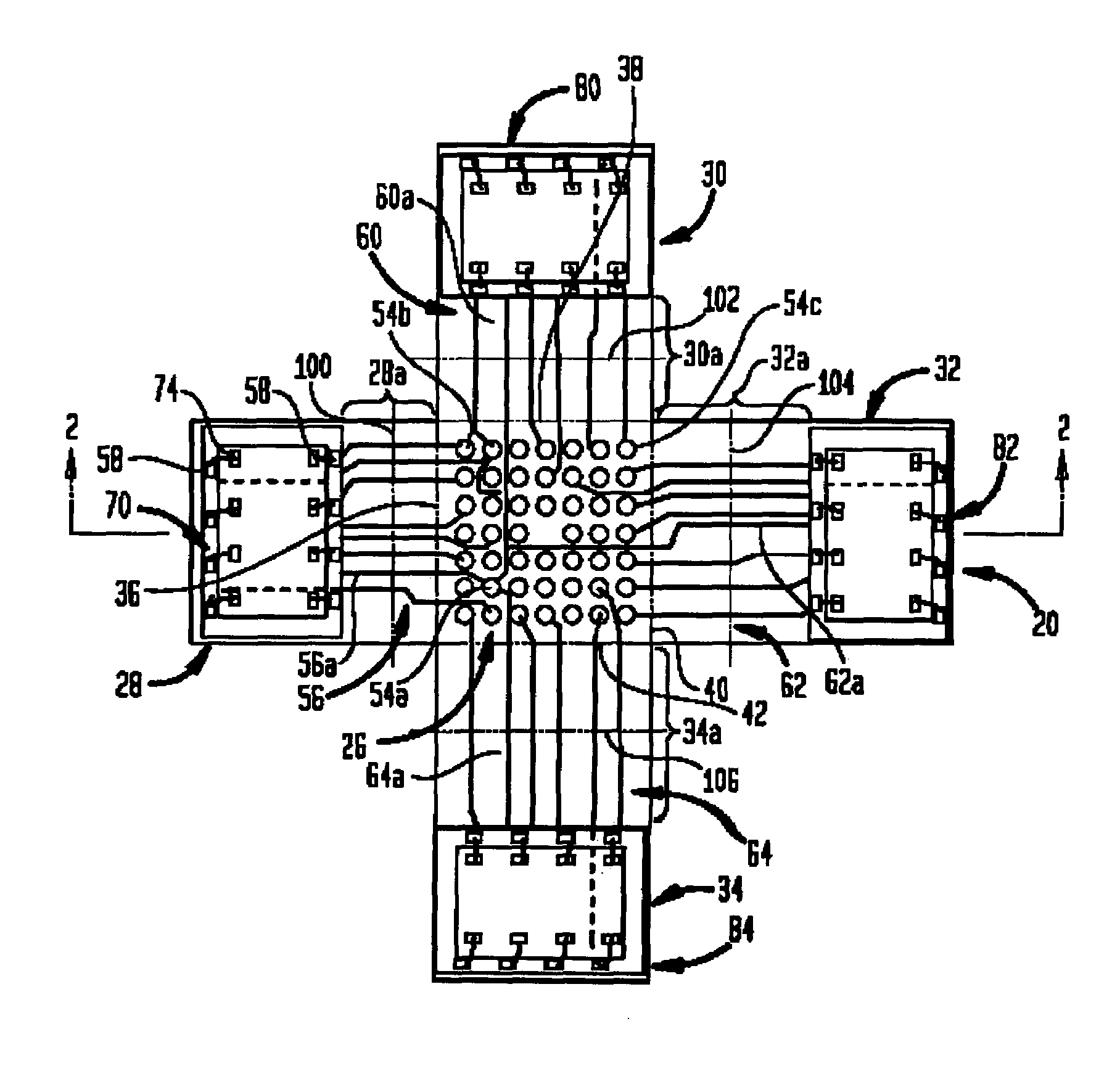
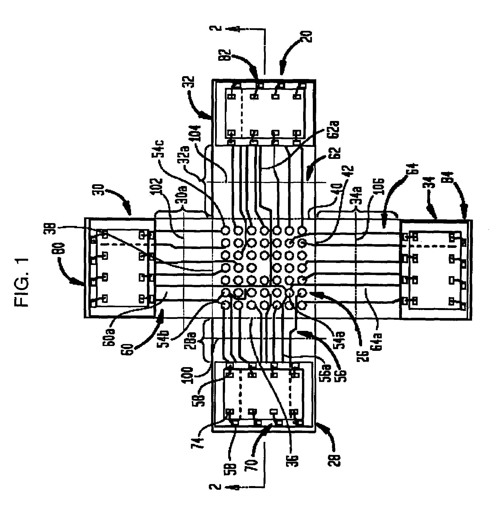
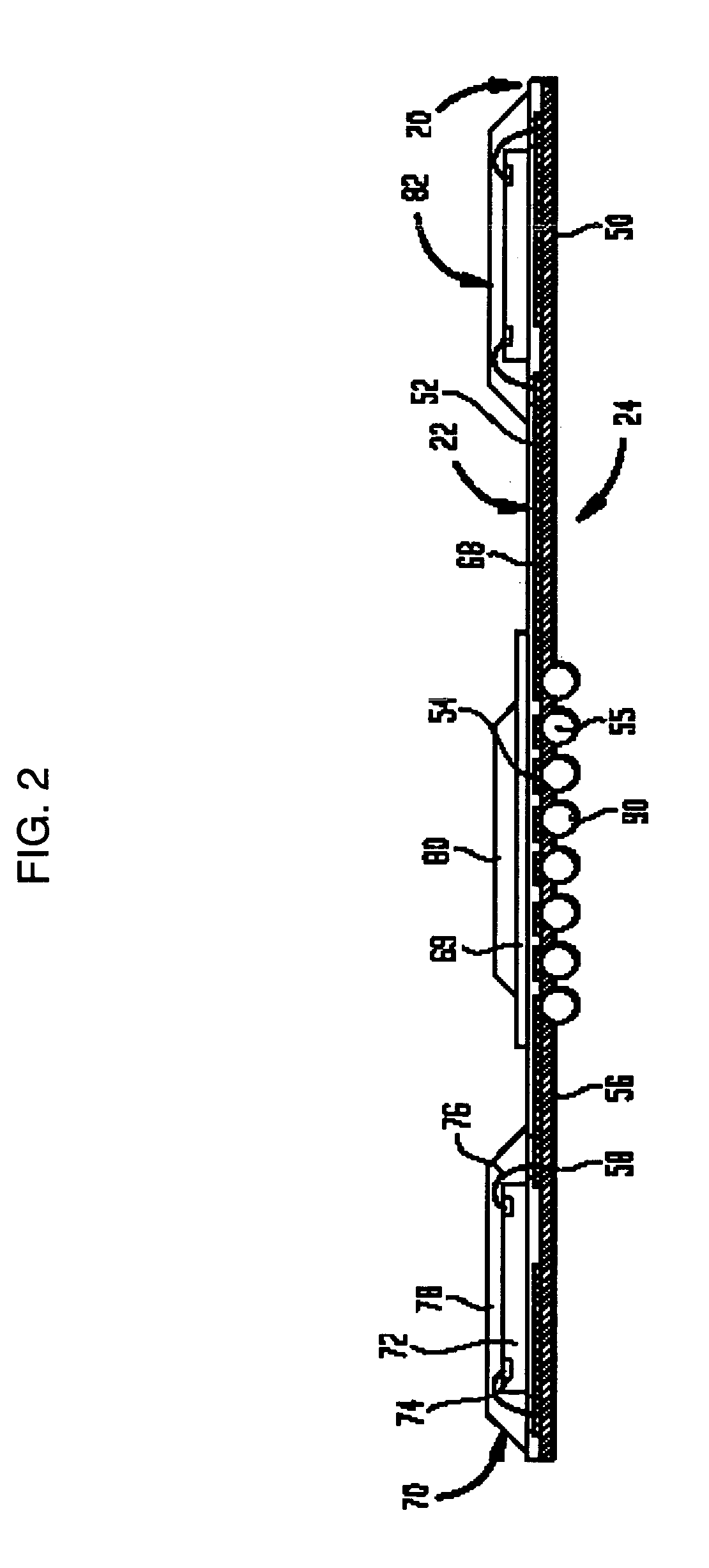
[0037]An assembly in accordance with one embodiment of the invention includes a component in the form of a unitary sheet 20. The sheet has a first or obverse side 22 (the side visible in FIG. 1) and oppositely-directed reverse side 24 (FIG. 2). The sheet is of generally cruciform shape as seen in plan view, and includes a square core panel 26 having edges 36, 38, 40 and 42. The unitary sheet further includes four side panels 28, 30, 32 and 34 projecting from the core panel at the four edges 36–42. The first side panel 28 includes a fold region 28a adjacent the first edge 36 of the core panel. Similarly, the second side panel 30 includes a fold region 30a adjacent edge 38 of the core panel, whereas the third side panel has a fold region 32a adjacent edge 40 of the core panel and the fourth side panel includes a fold region 34a adjacent the fourth edge 42 of the core panel. As described herein, the “length” of each side panel and fold region refers to the dimension of the side panel o...


PUM


Abstract

A stacked microelectronic assembly comprises a continuous sheet including a core panel and a plurality of side panels, each having a folded portion that connects the side panel to an edge of the core panel. At least two of the panels are at least partially horizontally aligned with one another in a stack. During manufacture of a stacked microelectronic assembly, failed microelectronic elements are identified and associated side panels thereof are simply cut-off. This results in the production of a usable stacked microelectronic assembly albeit of reduced capacity, or reduced functionality.

Description

CROSS-REFERENCE TO RELATED APPLICATION[0001]This application claims the benefit of U.S. Provisional Patent Application Ser. No. 60 / 409,880, filed Sep. 11, 2002, the disclosure of which is hereby incorporated by reference herein.BACKGROUND OF THE INVENTION[0002]The present invention relates to stacked microelectronic assemblies and methods of making such assemblies, to methods of forming such assemblies and to components useful in such assemblies.[0003]Semiconductor chips are commonly provided as individual, prepackaged units. A standard chip has a flat, rectangular body with a large front face having contacts connected to the internal circuitry of the chip. Each individual chip is mounted in a package, which in turn is mounted on a circuit panel, such as a printed circuit board, and which connects the contacts of the chip to conductors on the circuit panel. In many conventional designs, the chip package occupies an area of the circuit panel considerably larger than the area of the c...

Claims


Application Information

Patent Timeline
IPC IPC(8): H01L23/02H01L23/538H01L25/065H01L25/18
CPCH01L23/5387H01L25/0657H01L25/18H01L2924/07811H01L24/48H01L2924/3011H01L2224/48091H01L2224/48227H01L2225/06517H01L2225/06555H01L2225/06579H01L2225/06582H01L2924/01078H01L2924/01079H01L2924/15311H01L2924/19041H01L2924/30107H01L2924/00014H01L2924/00H01L2924/12042H01L2224/05599H01L2224/45099H01L2224/85399H01L2924/14H01L2924/181H01L2224/05553H01L2924/10161H01L2224/45015H01L2924/207H01L2924/00012
Inventor KANG, TECK-GYUKUBOTA, YOICHI
Owner TESSERA INC
Why Eureka
Try Eureka