Semiconductor output circuit device

a technology of output circuit and circuit device, which is applied in the direction of logic circuit coupling/interface arrangement, pulse technique, instruments, etc., can solve the problems of inability to transfer data at high speed, inability to supply power supply voltages vddq and vssq exclusively to the output circuit, and inability to accurately determine the logic level of received data. , to achieve the effect of generating an output signal/data of a small amplitude accurately and stably

Inactive Publication Date: 2006-07-11
RENESAS ELECTRONICS CORP
View PDF18 Cites 11 Cited by
  • Summary
  • Abstract
  • Description
  • Claims
  • Application Information

AI Technical Summary

Benefits of technology

[0045]An object of the present invention is to provide a semiconductor circuit device

Problems solved by technology

Thus, a subsequent circuit possibly may inaccurately determine the logic level of the received data, and the data cannot be transferred at high speed.
Thus, there is caused a problem that it is difficult to supply power supply voltages VDDQ and VSSQ exclusively to the output circuit.
That is, irrespective of whether or not data output is performed, amplitude limiting circuit 124 constantly flows the through-current, and current consumption, standby current in particular, would disadvantageously be increased.
In particular, if this semiconductor circuit device is a semiconductor memory device and outputs multibit data, the though-current further increases and semiconductor memory device cannot operate with low standby current.
If such variation factors as described above cause the ON res

Method used


Image

  • Semiconductor output circuit device
  • Semiconductor output circuit device
  • Semiconductor output circuit device

Examples


first embodiment

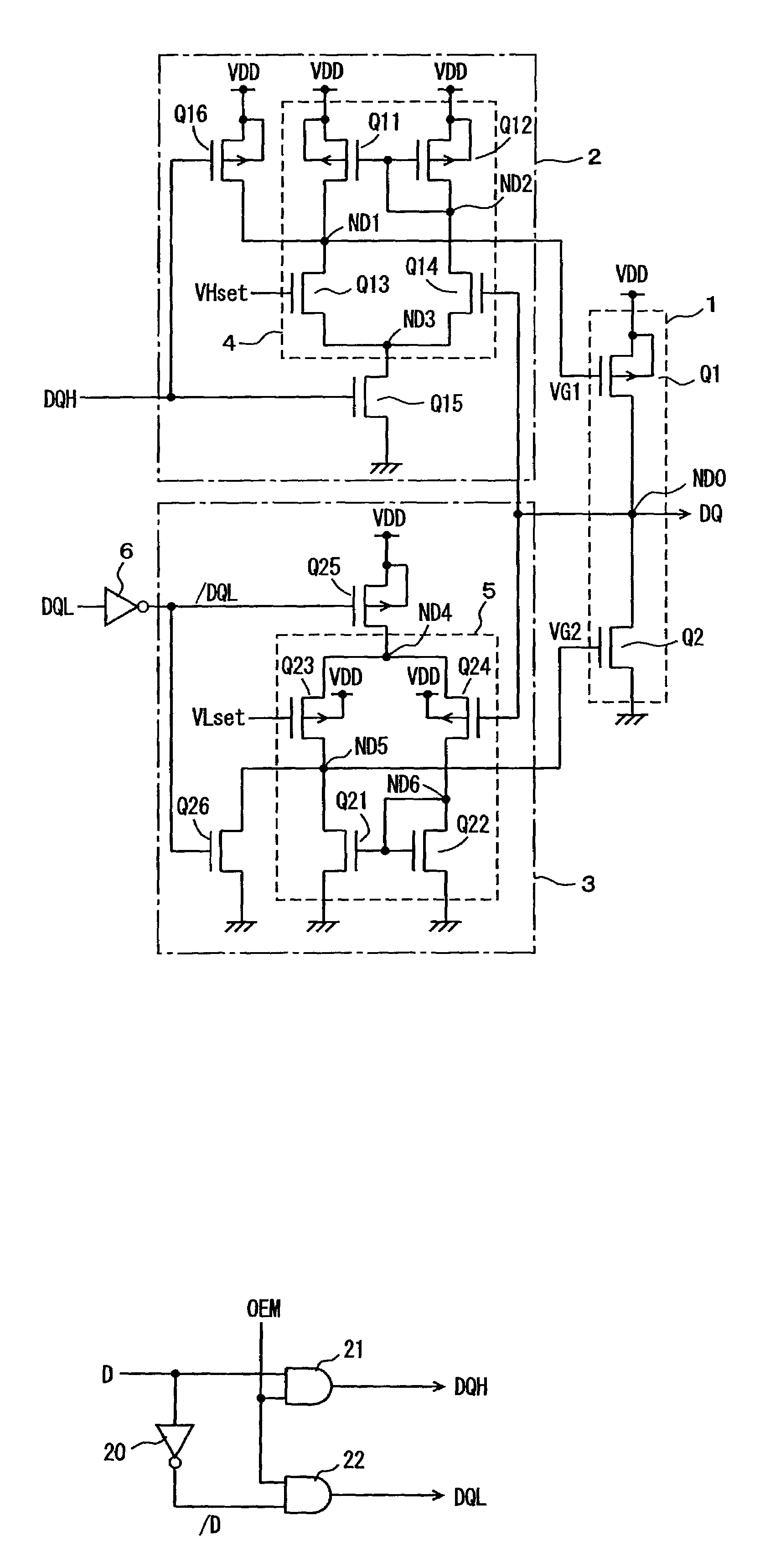
[0066]FIG. 1 shows a configuration of an output section of a semiconductor circuit device accordance with a first embodiment of the present invention. In FIG. 1, a data output node ND0 is driven in accordance with output control signals DQH and DQL output from an output drive control circuit 100 shown in FIG. 9. Although an operation of a data output section for outputting data DQ hereinafter, the output circuit according to the present invention can be a normal circuit for outputting a control signal, for example.

[0067]In FIG. 1, the data output circuit includes a comparison circuit 2 enabled when output control signal DQH is activated, to compare the voltage of output node ND0 with a reference voltage VHset, a comparison circuit 3 enabled when output control signal DQL is activated, to compare the voltage of output node ND0 with a reference voltage VLset, and an output buffer circuit 1 driving output node ND0 in accordance with the signals VG1 and VG2 output from comparison circui...

second embodiment

[0106]FIG. 4 shows a configuration of a semiconductor circuit device in accordance with a second embodiment of the present invention. In FIG. 4, the semiconductor circuit device includes a comparison circuit 11 enabled when output control signal DQH is activated, to compare the voltage of an output node ND11 with a reference voltage VHset1, to generate output drive control signal VG1 in accordance with the result of comparison, a comparison circuit 12 enabled when output control signal DQH is activated, to compare the voltage of output node ND11 with a reference voltage VHset2 to generate an output drive control signal VG3 in accordance with the result of comparison, a comparison circuit 13 enabled when output control signal DQL is activated, to compare the voltage of output node ND11 with a reference voltage VLset1 for generating an output drive control signal VG2 in accordance with the result of comparison, a comparison circuit 14 enabled when output control signal DQL is activate...


PUM


Abstract

Comparison circuits are provided, corresponding to a plurality of pull up transistors, each for comparing a voltage at an output node and each respective reference voltage different in voltage level from other, and for adjusting a drive current of a corresponding output pull up transistor, and further comparison circuits are provided, corresponding to a plurality of pull down transistors, each for comparing the voltage of the output node and each respective reference voltage different in voltage level from other, and each for adjusting an amount of a drive current of a corresponding pull down transistor in accordance with a result of comparison. The reference voltages each are set to a voltage level between a power supply voltage and a ground voltage. Without a dedicated power supply pin terminal, a signal of a small amplitude having the amplitude limited stably and precisely can be output at high speed.

Description

BACKGROUND OF THE INVENTION[0001]1. Field of the Invention[0002]The present invention relates generally to semiconductor circuit devices and particularly to semiconductor output circuit devices reliably generating an output signal at high speed.[0003]2. Description of the Background Art[0004]Semiconductor devices such as semiconductor memory devices and semiconductor logic processing devices need to use a bus for transmitting and receiving signals / data between devices. The bus signal line, provided external to the devices, has a large lord. In order to drive the external signal line at high speed for transferring a signal / data, these semiconductor devices are each provided with an output circuit formed of a transistor having a large driving capability. With an output circuit for transferring a signal / data, the bus signal line needs to be driven to an H (logical high) level or an L (logical low) level depending on the signal / data to be transmitted.[0005]FIG. 9 shows an exemplary conf...

Claims


Application Information

Patent Timeline
IPC IPC(8): H03K5/153G11C11/417H03K19/00H03K19/017H03K19/0175
CPCH03K19/01707H03K19/0013H03K19/01721H03K19/017
Inventor KAJIMOTO, TAKESHI
Owner RENESAS ELECTRONICS CORP
Why Eureka
Try Eureka