Display panel drive circuit and plasma display

a drive circuit and display panel technology, applied in the field of display panel drive circuit and plasma display, can solve the problems of increasing power consumption, reducing the effect of power reduction, and greatly losing the effect of reducing power consumption, so as to reduce the parasitic inductance of the resonant current path, reduce the resonance cycle, and shorten the wire length of the resonant circuit

Inactive Publication Date: 2006-07-11
HITACHI LTD
View PDF22 Cites 10 Cited by
  • Summary
  • Abstract
  • Description
  • Claims
  • Application Information

AI Technical Summary

Benefits of technology

[0038]The resonant circuit is provided for each one or plurality of the second switching elements so that wire length of the resonant circuit is shortened and parasitic inductance of a resonant current path can be reduced. This realizes high-speed drive with a reduced resonance cycle and reduction in power consumption as a result of improvement in power recovery efficiency due to increase in the Q value. Further, by reducing the number of the first switching element having small effects on resonance, circuit costs can be reduced.

Problems solved by technology

The conventional drive circuit shown in FIG. 20 described above intends to reduce power consumption through the use of the resonant phenomenon, but there is a problem that an effect of reducing power consumption is greatly lost as the recent plasma display panel has higher resolution and larger size.
At this time, only values of the resonant inductances provided in the power recovery circuit need to become smaller, which decreases the effect of power reduction due to decrease in Q of the resonance.
Furthermore, as the output frequency of the drive circuit is increased, the number of times the plasma display panel is driven by a high-voltage pulse is also increased, which increases power consumption and causes a big problem of heating in the drive circuit (the drive IC).
If power consumption of the drive circuit 3 cannot be reduced sufficiently, heatsinking costs and parts costs of each part in the display are increased.
Further, there may arise a case in which light-emission brightness is restricted by heatsinking limitation of the display device itself or downsizing as an advantage of a flat panel display is not realized sufficiently.

Method used


Image

  • Display panel drive circuit and plasma display
  • Display panel drive circuit and plasma display
  • Display panel drive circuit and plasma display

Examples


first embodiment

[0060

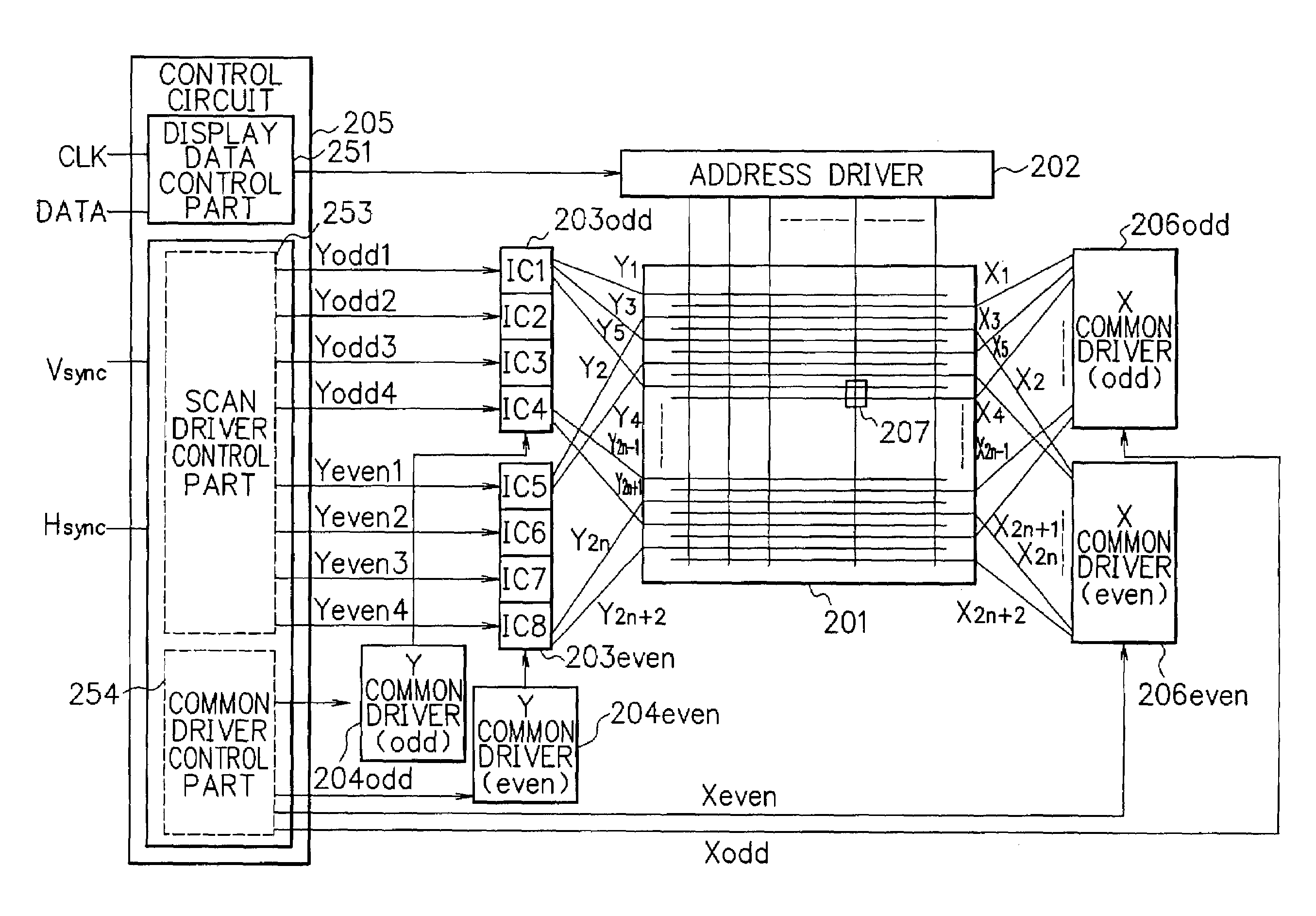
[0061]FIG. 1 shows a block diagram of an overall configuration of a plasma display device according to a first embodiment of the present invention. This plasma display device can reduce a load capacitance of a panel drive circuit. This plasma display device is composed of a plasma display panel 201, a control circuit 205 which forms a control signal for controlling a drive circuit of the display panel by an interface signal which is inputted from the outside, X common drivers (X electrode drive circuits) 206odd and 206even, scan electrode drive circuits (scan drivers) 203odd and 203even, Y common drivers 204odd and 204even for driving panel electrodes by the control signal from the control circuit 205, and an address electrode drive circuit (address driver) 202.

[0062]The X common drivers 206odd and 206even generate a sustain voltage pulse. The Y common drivers 204odd and 204even also generate a sustain voltage pulse. The scan drivers 203odd and 203even independently drive and s...

second embodiment

[0092

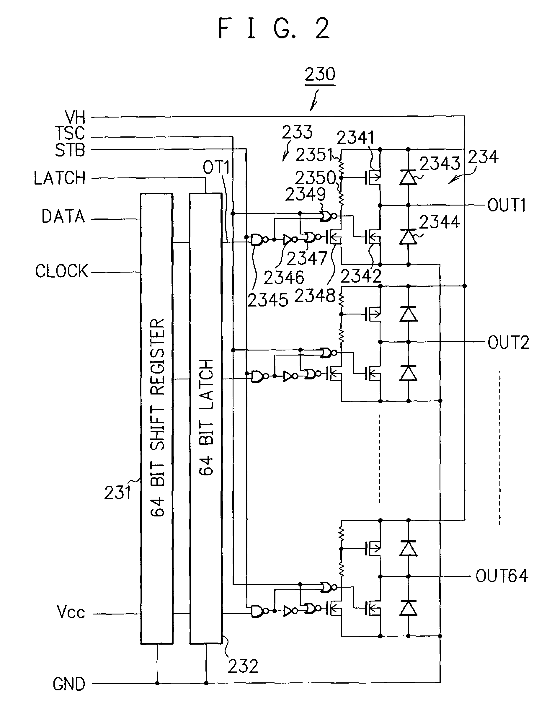
[0093]FIG. 5 shows a configuration of the address driver 202 according to a second embodiment of the present invention. Although the two drive elements 6 and 7 are used in FIG. 21, a single drive element 6 is used in the address drive in FIG. 5 so that power consumption (heating) can be reduced while circuit costs are cut.

[0094]In a drive power supply 1, a reference terminal 9 is connected to a reference potential (ground) 4. A drive circuit 3 has the drive element 6, a power supply terminal 8 connected to a power supply terminal 11 of the drive power supply 1, and an output terminal 10 connected to the address electrode of the plasma display panel 201 (FIG. 1). A resistance 2 and a capacitance 5 are a resistance and a capacitance of the address electrode and have a resistance value RL and a capacitance value CL respectively.

[0095]Properly speaking, a load such as a drive electrode for a flat display panel like the plasma display panel has the structure in which a parasitic cap...

third embodiment

[0123

[0124]FIG. 12A shows a configuration example of the address driver 202 (FIG. 1) according to a third embodiment of the present invention. This address driver 202 can reduce power consumption by reusing electric charge, which is charged in a load capacitance, when output is changed over.

[0125]A power supply terminal 8 of a drive circuit 3 is connected to a drive power supply 1 via a switching circuit 80. P-channel MOSFETs 601a, 601b, and 601c have parasitic diodes 602a, 602b, and 602c respectively, sources connected to the power supply terminal 8, and drains connected to output terminals 10a, 10b, and 10c respectively. Anodes and cathodes of the parasitic diodes 602a to 602c are connected to drains and sources of the FETs 601a to 601c respectively. Gates of the FETs 601a to 601c are connected to an output of a drive circuit 600.

[0126]N-channel MOSFETs 701a, 701b, and 701c have parasitic diodes 702a, 702b, and 702c respectively, sources connected to a ground terminal 4, and drain...


PUM


Abstract

A display panel drive circuit having a plurality of first and second electrodes for connecting to a display panel, a first drive circuit for driving the first electrodes, and a second drive circuit for driving the second electrodes. The second drive circuit is connected to drive all or a part of a plurality of the second electrodes, or interrupted to increase output impedance.

Description

CROSS-REFERENCE TO RELATED APPLICATIONS[0001]This application is based upon and claims priority of Japanese Patent Application No. 2002-024493, filed on Jan. 31, 2002, the contents being incorporated herein by reference.BACKGROUND OF THE INVENTION[0002]1. Field of the Invention[0003]The present invention relates to a circuit for driving a display panel, particularly to a circuit configuration capable of reducing power consumption in driving a display panel for a plasma display, an electroluminescence display, a liquid crystal display (LCD), or the like, as a capacitive load, and relates to a display device to which the drive circuit is applied.[0004]2. Description of the Related Art[0005]FIG. 15 is a block diagram schematically showing a three-electrode surface-discharge plasma display panel of an AC drive type, and FIG. 16 is a cross sectional view for explaining the electrode structure of the plasma display panel shown in FIG. 15. In FIG. 15 and FIG. 16, the reference numeral 207 ...

Claims


Application Information

Patent Timeline
Patent Type & Authority Patents(United States)
IPC IPC(8): G09G5/00G09G3/20G09G3/288G09G3/291G09G3/294G09G3/296G09G3/298
CPCG09G3/296G09G3/2965G09G2330/021G09G2310/0289
Inventor SANO, YUJIKAWADA, TOYOSHI
Owner HITACHI LTD
Why Eureka
Try Eureka