
System and method for calibrating signal paths connecting a device under test to a test system

a signal path and signal path technology, applied in the field of system and method for calibrating signal paths connecting a device under test to a test system, can solve the problems of circuit manufacturers, complex integrated circuits, faster and more efficient integrated circuits, etc., and achieve the effect of enhancing the precision of signal timing measurements and facilitating the development of increasingly faster integrated circuits

Inactive Publication Date: 2006-07-11
GUIDE TECH
View PDF15 Cites 19 Cited by
  • Summary
  • Abstract
  • Description
  • Claims
  • Application Information

AI Technical Summary

Benefits of technology

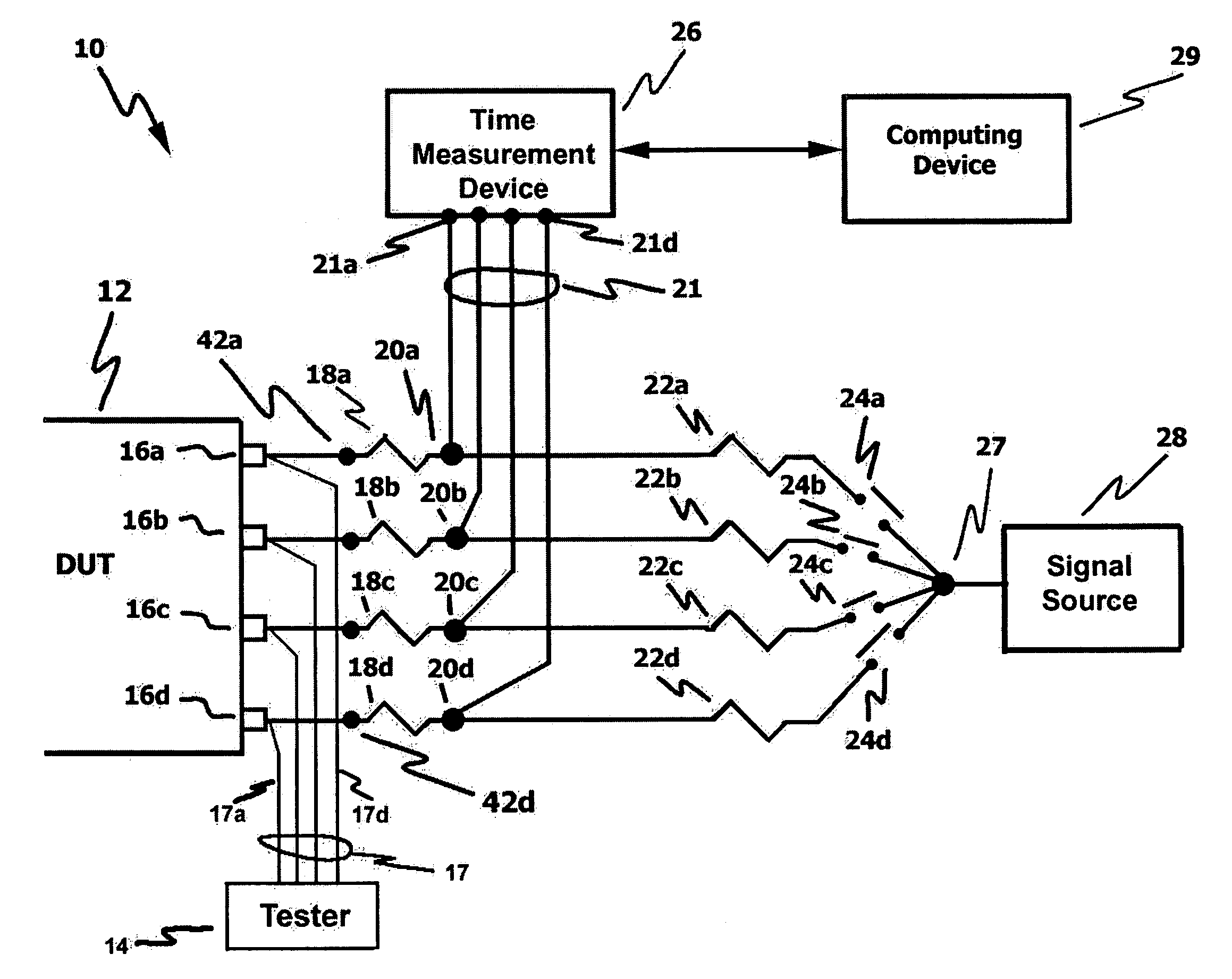
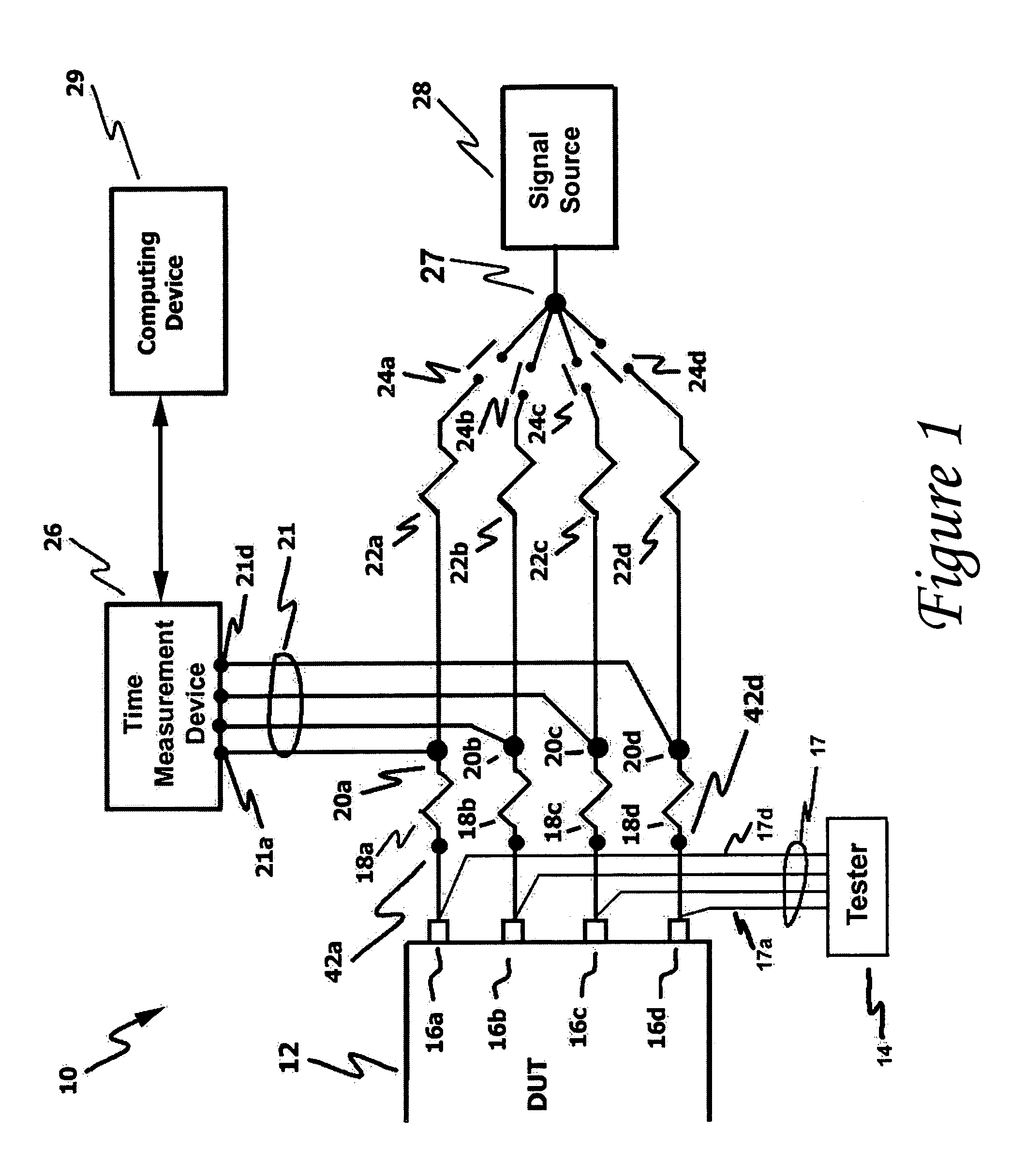
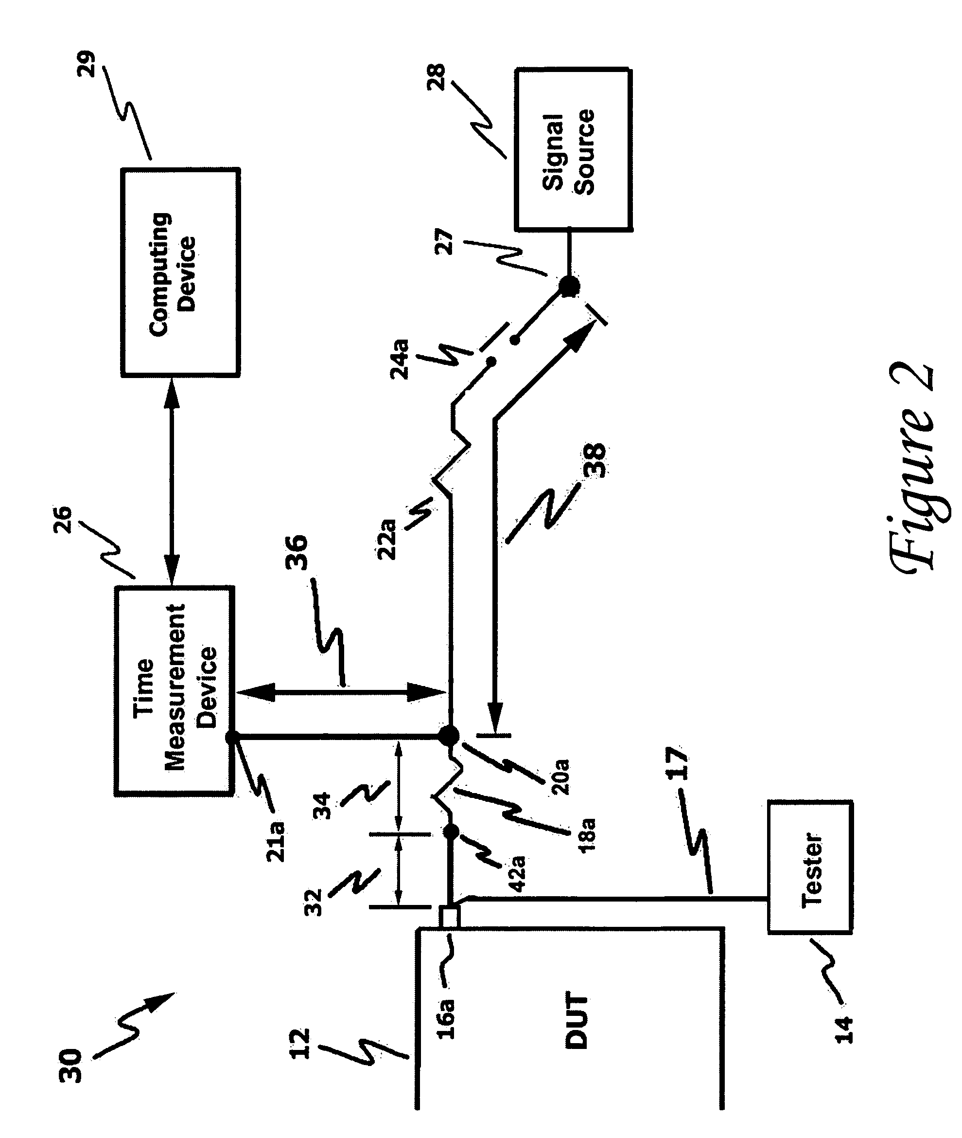
"The patent text describes an improved calibration system and method for signal timing in test systems. The system uses a calibration circuit with sampling resistors and isolation resistors to measure signal skew between different signals in a device under test. The calibration circuit is placed close to the device under test to ensure accurate measurements. The system also includes a loadboard with integrated calibration capabilities for automated testing equipment. The method involves injecting a calibration signal into each signal path and measuring the skew of all signals relative to a reference channel. The system and method can be used to calibrate signal paths in high-speed integrated circuits and detect defects in mass-produced circuits."

Problems solved by technology

The complexity of integrated circuits ranges from simple logic gates and memory units to large arrays capable of complete video, audio and print data processing.
The demand for faster and more efficient integrated circuits, however, has created various problems for circuit manufacturers.
No manufacturing process is perfect and manufacturing imperfections in an integrated circuit may cause timing irregularities such as pulse-width deviation errors, to name only one type.
Conventional ATE systems are not always capable of providing comprehensive measurements of integrated circuit I / O signals when such circuits operate at increasingly higher frequencies, such as those on an order of about 10 MHz–1 GHz or higher.
Lack of such synchronization between signals is called skew.

Method used


Image

  • System and method for calibrating signal paths connecting a device under test to a test system
  • System and method for calibrating signal paths connecting a device under test to a test system
  • System and method for calibrating signal paths connecting a device under test to a test system

Examples


Embodiment Construction

[0019]As previously discussed, the present technology relates to a method and apparatus for precision calibration of two or more distinct signal paths in a test setup. A signal path calibration system in accordance with the disclosed technology measures the signal skew associated with each distinct signal path connecting a device under test (DUT), such as an integrated circuit, to a time measurement device (TMD), such as a time interval analyzer. Signal skew measurements may be performed at selected times in conjunction with a DUT testing process. In addition, the measured skew values may be stored by the TMD. Such skew values may be used as needed to enhance the accuracy of DUT timing measurements by adjusting subsequent test signal timing measurements to compensate for skew between signal paths. Such stored skew values may also be used by a computing device to provide statistical analysis for signal path failure detection.

[0020]It should be noted that each of the exemplary embodim...


PUM


Abstract

The present technology involves an apparatus and method for calibrating a plurality of distinct signal paths connecting a device under test (DUT) to a time measurement device. The disclosed calibration circuit, which may be connected to the test setup throughout the testing process, measures the signal skew associated with each distinct signal path connecting a DUT, such as an integrated circuit, to a time measurement device, such as a time interval analyzer. The measured skew values, which may be collected throughout the testing process, are stored in memory. Such memory may be within the time measure device, an external storage device or a computing device that may be in communication with the time measurement device. The time measurement device uses the stored skew values to adjust the test signals to compensate for signal path related signal skew. In addition, the stored skew values are used to perform signal path diagnostics. This is accomplished by comparing newly measured skew values to stored skew values and generating a signal path failure signal when the newly measured skew values fall outside a user programmable range of acceptable skew values.

Description

BACKGROUND OF THE INVENTION[0001]The present technology relates to a method and apparatus for measuring the signal skew associated with each distinct signal path connecting a device under test (DUT), such as an integrated circuit or other electronic device, and associated tester equipment to a time measurement device, such as a time interval analyzer.[0002]In general, an integrated circuit refers to an electrical circuit contained on a single monolithic chip containing active and passive circuit elements. As should be well understood in this art, integrated circuits are fabricated by diffusing and depositing successive layers of various materials in a pre-selected pattern on a substrate thereby imprinting a complex of electronic components and their interconnections. Materials used to manufacturer integrated circuits can include semiconductive materials such as silicon, conductive materials such as metals, and low dielectric materials such as silicon dioxide. The semiconductive mate...

Claims


Application Information

Patent Timeline
Patent Type & Authority Patents(United States)
IPC IPC(8): G01D18/00G01R31/00
CPCG01R31/31905G01R31/31937G01R31/3191
Inventor HORNE, STEPHEN JOHNALIG, JOSEPH
Owner GUIDE TECH
Learn More