Structure, structure manufacturing method and sensor using the same

a manufacturing method and sensor technology, applied in the field of structure manufacturing method and sensor using the same, can solve the problems of lowering the reliability of the sensing device and the difficulty of fabrication, and achieve the effect of improving and stabilizing the sensitivity of the sensor

Inactive Publication Date: 2006-07-18
FUJIFILM CORP
View PDF9 Cites 54 Cited by
  • Summary
  • Abstract
  • Description
  • Claims
  • Application Information

AI Technical Summary

Benefits of technology

[0011]The invention has been made in consideration of the circumstances and has an object to provide a structure in which metallic particles can be arranged regularly with an optional uniform size in an optional array, a method of manufacturing the structure and a sensor using the same, and furthermore, to enhance and stabilize a sensor sensitivity when the structure is to be used as the sensor and to provide a novel use of only a novel structure.
[0013]In the structure, the metallic particles are formed in the pore of the anodic oxidized alumina capable of comparatively freely controlling a pore size, a pore spacing and a pore depth, and the metallic particles can be fabricated with an optional uniform size and can be regularly arranged easily. Consequently, the metallic particles can be arranged at a higher density, and the sensor sensitivity of a device can be enhanced and the sensitivity can be stabilized when the structure is to be used as the sensor. Furthermore, it is possible to provide a novel use of only a novel structure.
[0017]In the method of manufacturing the structure, the anodic oxidized alumina having the independent pores arranged at almost regular intervals in an almost vertical direction with respect to the layer plane is coated with the metal. Consequently, the respective pores can be filled with the metal. Then, the metal coated film formed on the opening surface of the independent pore of the anodic oxidized alumina is removed so that the metals coated and filled in the independent pores remain in an isolation state from each other. As a result, the metallic particles which are independent of each other are arranged at regular intervals and a high density.

Problems solved by technology

However, it is hard to carry out fabrication with the metallic particles having a uniform size and to regularly arrange the metallic particles.
Further, when dispersion in the sizes or the shapes are occurring over a plurality of the sensing devices, it raises another problem, namely difficulty for determining whether the measured absorbance or resonance wave length are obtained from changes made in refractive index, or said dispersion in the sizes or the shapes, which might end up lowering its reliability of the sensing devices.

Method used


Image

  • Structure, structure manufacturing method and sensor using the same
  • Structure, structure manufacturing method and sensor using the same
  • Structure, structure manufacturing method and sensor using the same

Examples


first embodiment

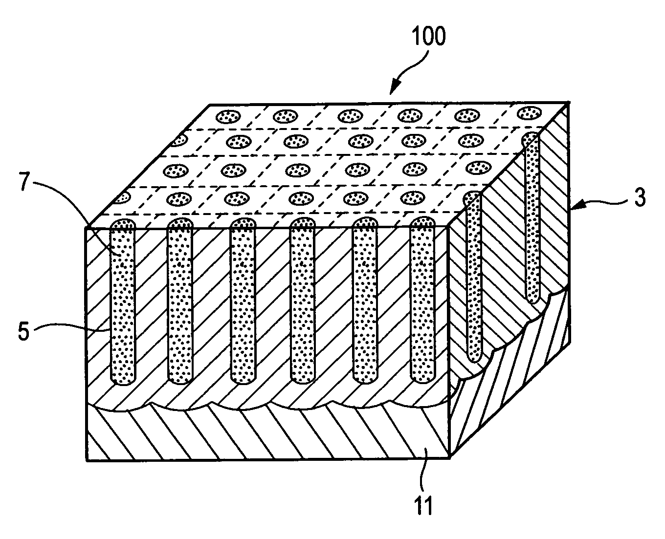
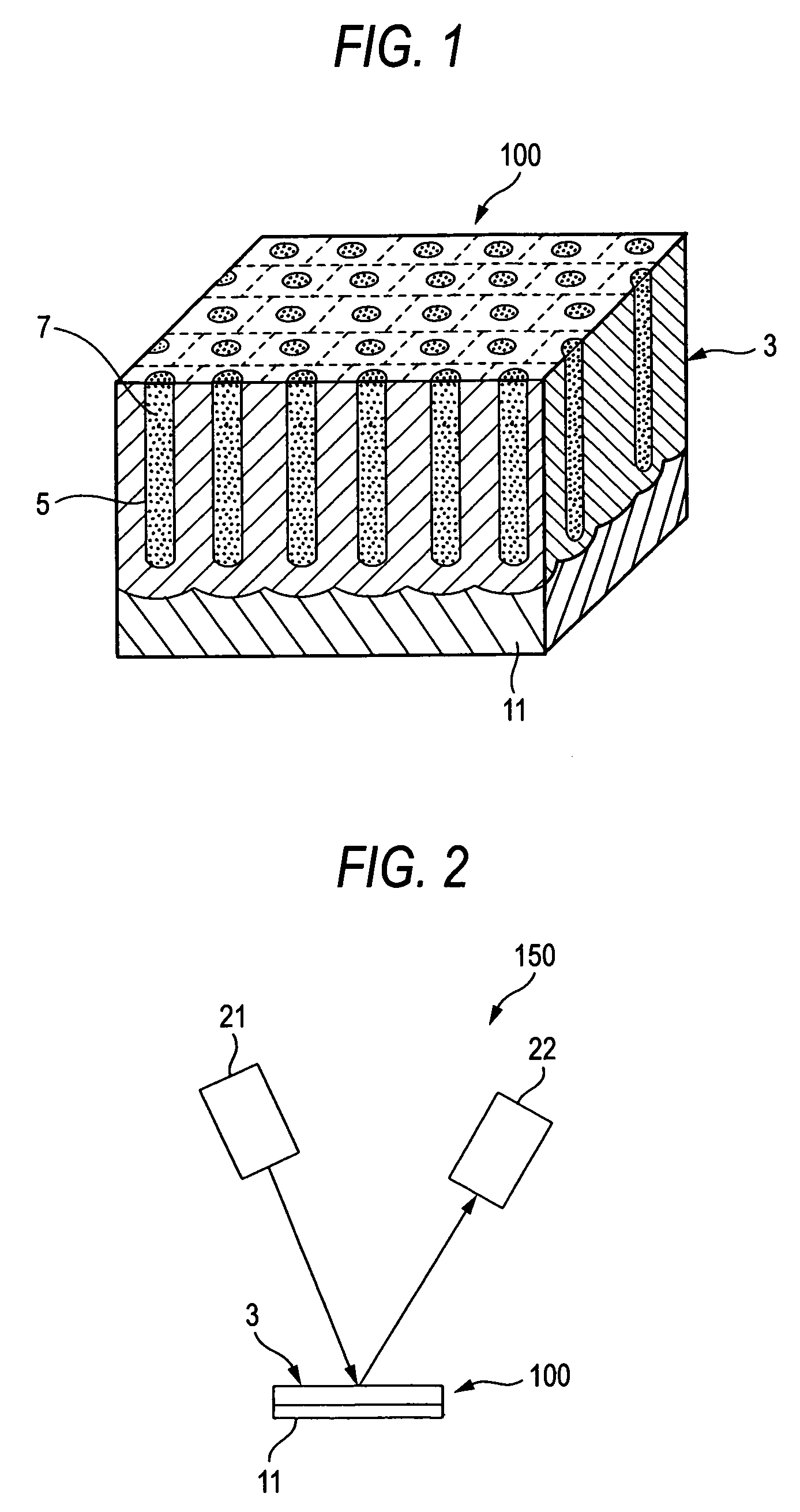
[0030]FIG. 1 is a perspective view showing a main part according to the structure in accordance with the invention and FIG. 2 is a view illustrating a state in which a measurement is carried out by using the structure as the sensor.

[0031]In a plasmon resonance device 100 according to an example of the structure in accordance with the invention, a metallic particle 7 is filled in each of a plurality of pores 5 of anodic oxide alumina 3 formed like a layer and a metallic particle dispersing element having the metallic particles isolated from each other is thus formed.

[0032]A method of manufacturing the anodic oxidized alumina 3 will be described below and the anodic oxidized alumina 3 has the pores 5 formed at almost regular intervals in an almost vertical direction with respect to a layer plane. In other words, the pores are provided regularly in the layer. For this reason, the metallic particles 7 filled in the pore 5 are isolated from each other and are provided regularly as a whol...

second embodiment

[0058]Next, the structure according to the invention will be described.

[0059]FIG. 8 is a sectional view showing the construction of a structure plasmon resonance device (structure) according to the embodiment. The same members as those shown in FIG. 1 have the same reference numerals and repetitive description will be omitted.

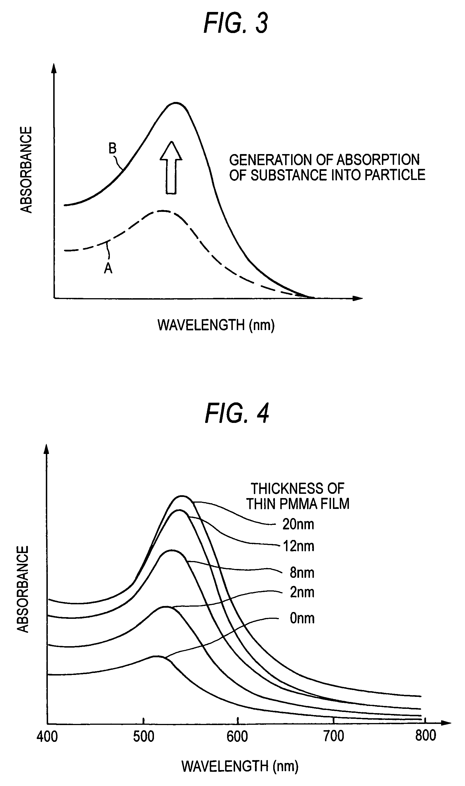
[0060]A plasmon resonance device 300 according to the embodiment has a hollow portion 23 which is not filled with a metal (gold) in the bottom portion of a pore 5. Other structures are the same as those of the plasmon resonance device 100 according to the first embodiment.

[0061]Also in the plasmon resonance device 300 thus constituted, a light beam is irradiated on the plasmon resonance device 300 from a light source and the absorbing spectrum of light reflected from or transmitted through the plasmon resonance device 300 is measured by a spectrophotometer to obtain an absorbance so that a change in the refractive index of a medium in the vicinity of the surfac...


PUM

PropertyMeasurementUnit
diameteraaaaaaaaaa
diameteraaaaaaaaaa
refractive indexaaaaaaaaaa

Abstract

A plasmon resonance device 100 according to an example of a structure is characterized in that metallic particles 7 isolated from each other are formed in each of a plurality of pores 5 of anodic oxidized alumina 3. As a method of manufacturing the plasmon resonance device 100, a metal is coated on the anodic oxidized alumina 3 opening the pores 5 and a metal coated element provided on the opening surface of the pore in the anodic oxidized alumina 3 is removed. Consequently, metallic particles isolated from each other are formed in the respective independent pores. The plasmon resonance device 100 can be used as a sensor utilizing a localized plasmon resonance phenomenon.

Description

[0001]This is a divisional of application Ser. No. 10 / 329,334 filed Dec. 27, 2002.BACKGROUND OF THE INVENTION[0002]1. Field of the Invention[0003]The present invention relates to a structure mainly applying a localized plasmon resonance phenomenon, a method of manufacturing the structure and a sensor using the same, and more particularly to a technique for arranging metallic particles for inducing a plasmon resonance at a high density.[0004]2. Description of the Related Art[0005]Referring to a metal dot, such as formed by gold or silver with a smaller size being smaller than the wavelength of light, occurring a localized plasmon resonance is well known, and a device making use of said phenomenon is also known. Forming a metal colloid monolayer film is known as a method of forming such a device. For example JP-A2000-356587 has disclosed one of the utilizations of the properties. In this publication, metallic particles are fixed like a film on the surface of a substrate formed by an o...

Claims


Application Information

Patent Timeline
Patent Type & Authority Patents(United States)
IPC IPC(8): G01N21/55G01B9/02C12M1/34G01N33/553
CPCG01N21/554
Inventor MUKAI, ATSUSHI
Owner FUJIFILM CORP
Why Eureka
Try Eureka