
Multiband data communication apparatus, communication method of multiband data communication apparatus, and storage medium

a multi-band data communication and multi-band technology, applied in the field of multi-band data communication apparatus, can solve the problems of deteriorating signal quality of low-noise baseband signal, inability to establish frequency relationship, etc., and achieve the effect of avoiding deterioration of reception baseband signal and transmission baseband signal

Inactive Publication Date: 2006-07-18
PANASONIC CORP
View PDF13 Cites 36 Cited by
  • Summary
  • Abstract
  • Description
  • Claims
  • Application Information

AI Technical Summary

Benefits of technology

[0031]The present invention has been made to solve the above-described problems, and therefore, has an object to provide a multiband data communication apparatus, and a communication method of a multiband data communication apparatus, capable of suppressing a circuit scale of an additionally provided circuit to a minimum circuit scale, which is suitably constituted in an integrated circuit form, while switching a plurality of frequency bands in response to a band switching signal and furthermore, while a deterioration in a baseband signal is avoided. Another object of the present invention is to provide a storage medium for storing thereinto a computer readable program used to execute the communication method of the multiband data communication apparatus.
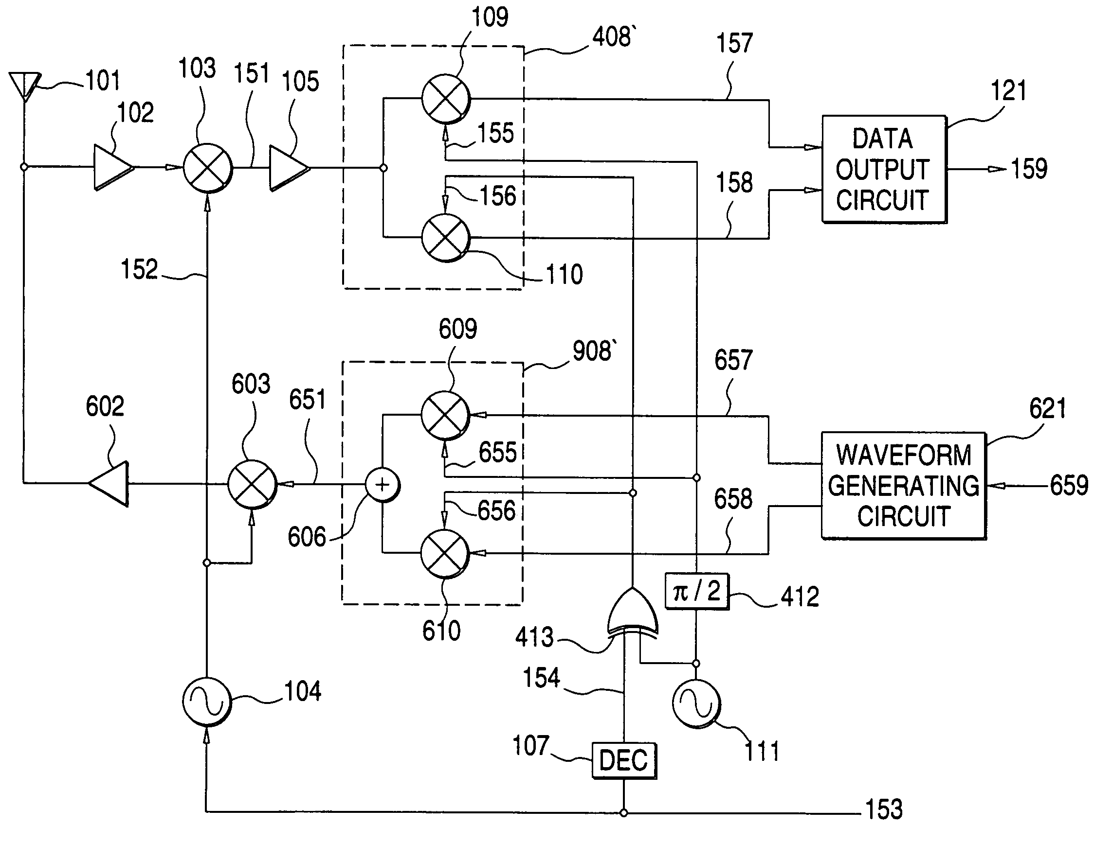
[0053]As a result, the correct reception baseband signal is obtained not depending upon the frequency band, but a desirable reception baseband signal can be obtained irrespective of the frequency relationship between the reception signal and the local oscillation signal, and then the correct demodulating process operation can be carried out in accordance with the band switching control by the band switching signal. To this end, only the phase shifting means (phase shifting step) is additionally provided as the structural element (processing step). The increase in the additionally provided circuit scale (processing step) can be suppressed to the minimum circuit scale, as compared with the conventional arrangement in which the polarity of the reception baseband signal itself is switched by the data output circuit. Therefore, such an arrangement may be suitably formed in an integrated circuit. Furthermore, since the correct demodulating process operation can be carried out in accordance with the band switching control by receiving the band switching signal, the deterioration of the reception baseband signal can be avoided. To the contrary, conventionally, the reception baseband signal is directly processed to invert the code polarities of the quadrature components.
[0055]As a result, the correct transmission signal is obtained not depending upon the frequency band, but a desirable transmission signal, or a desirable transmission intermediate frequency signal can be obtained irrespective of the frequency relationship between the transmission signal and the local oscillation signal, and then the correct modulating process operation can be carried out in accordance with the band switching control by the band switching signal. To this end, only the phase shifting means (phase shifting step) is additionally provided as the structural element (processing step). The increase in the additionally provided circuit scale (processing step) can be suppressed to the minimum circuit scale, as compared with the conventional arrangement in which the polarity of the transmission baseband signal itself is switched by the waveform generating circuit. Therefore, such an arrangement may be suitably formed in an integrated circuit. Furthermore, since the correct demodulating process operation can be carried out in accordance with the band switching control by receiving the band switching signal, the deterioration of the transmission baseband signal can be avoided. To the contrary, conventionally, the transmission baseband signal is directly processed to invert the code polarities of the quadrature components.
[0057]As a result, the correct reception baseband signal and the correct transmission signal can be obtained not depending upon the frequency band, but the correct modulating / demodulating process operations can be carried out in accordance with the band switching control by the band switching signal. To this end, only the phase shifting means (phase shifting step) is additionally provided as the structural element (processing step) in the transmission system and the reception system. The increase in the additionally provided circuit scale (processing step) can be suppressed to the minimum circuit scale, as compared with the conventional arrangement in which the polarity of the reception baseband signal itself is switched by the data output circuit, and also the polarity of the transmission baseband is switched by the waveform generating circuit. Therefore, such an arrangement may be suitably formed in an integrated circuit. Furthermore, since the correct demodulating process operation can be carried out in accordance with the band switching control by receiving the band switching signal, the deteriorations of the reception baseband signal and the transmission baseband signal can be avoided. To the contrary, conventionally, the reception baseband signal and also the transmission baseband signal are directly processed to invert the code polarities of the quadrature components.
[0065]As previously explained, the structural element (processing step) additionally provided so as to execute the correct modulating / demodulating process operations in accordance with the band switching control by the band switching signal may be realized by, for example, a DDS (Direct Digital Synthesizer) and a DSP (Digital Signal Processor) and the like, which are additionally provided in the transmission system and the reception system. As a consequence, the increase in the additionally provided circuit scale (processing step) can be suppressed to the minimum circuit scale, as compared with the conventional arrangement in which the polarity of the transmission baseband signal is switched by the waveform generating circuit, and the polarity of the reception baseband signal is changed by the data output circuit. Therefore, such an arrangement may be suitably formed in an integrated circuit. Furthermore, since the correct demodulating process operation can be carried out in accordance with the band switching control by receiving the band switching signal, the deteriorations of the reception baseband signal and the transmission baseband signal can be avoided. To the contrary, conventionally, the transmission baseband signal and the reception baseband signal are directly processed to invert the code polarities of the quadrature components.

Problems solved by technology

However, such a frequency relationship cannot always be established in such a circuit arrangement capable of handling a plurality of frequency bands called as either “dual band” or “multiband”.
Moreover, there is another problem that since such a circuit is additionally provided, the signal quality of such a low-noise baseband signal would be deteriorated.

Method used


Image

  • Multiband data communication apparatus, communication method of multiband data communication apparatus, and storage medium
  • Multiband data communication apparatus, communication method of multiband data communication apparatus, and storage medium
  • Multiband data communication apparatus, communication method of multiband data communication apparatus, and storage medium

Examples


first embodiment

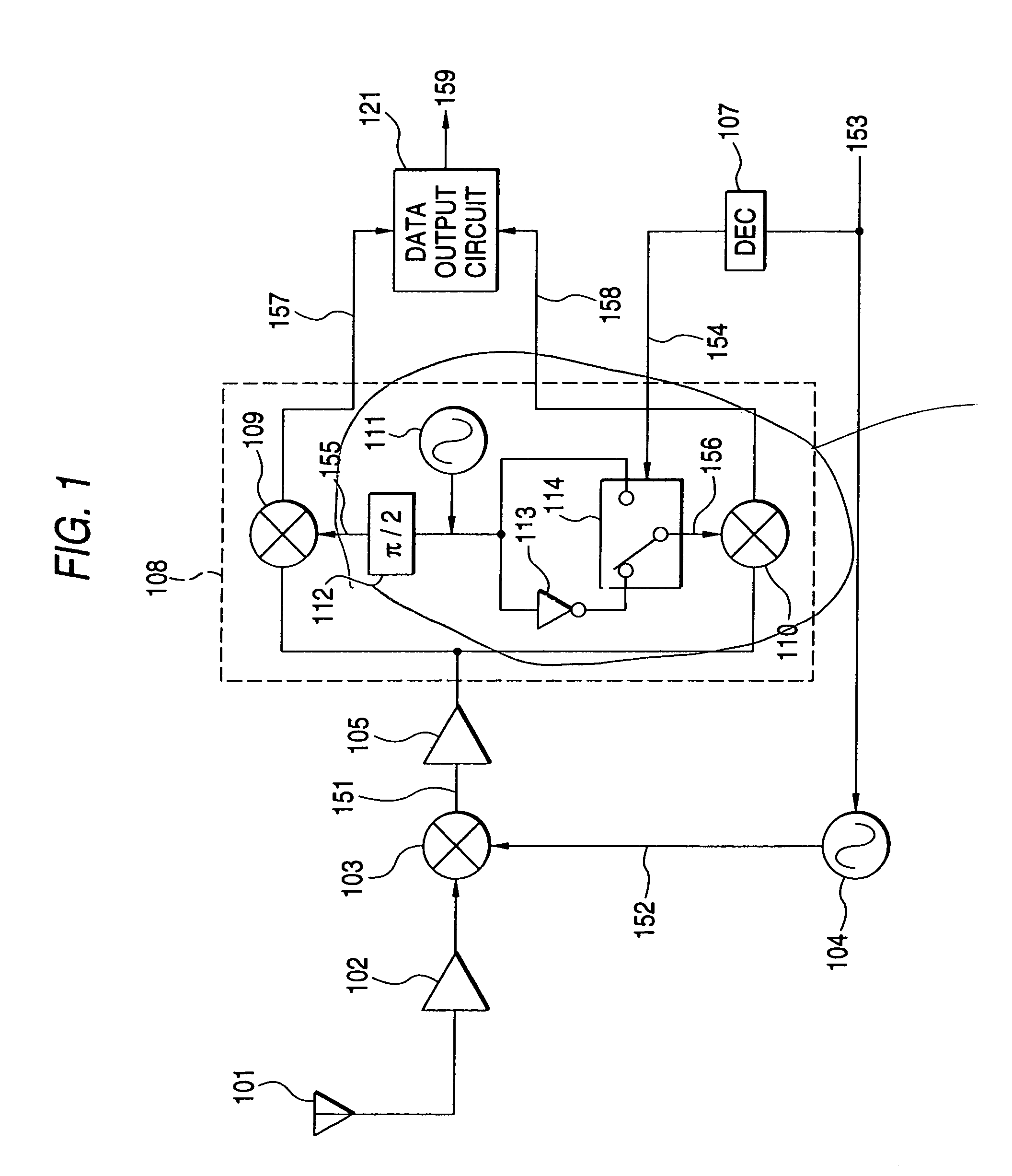
[0080]FIG. 1 is a structural diagram for indicating either a multiband data communication apparatus or a multiband data communication apparatus to which a communication method is applied, according to a first embodiment mode of the present invention. This first embodiment mode is such a multiband data communication apparatus for receiving by switching a plurality of frequency bands in response to a band switching signal, namely is directed to a data communication apparatus such as a mobile communication apparatus which is typically known as a digital portable telephone and a paging receiver.

[0081]In FIG. 1, the multiband data communication apparatus, according to this first embodiment mode, is arranged by employing an antenna 101, an radio frequency amplifier 102, a downconverter 103, a local oscillator 104, an intermediate frequency amplifier 105, a quadrature demodulator 108, and also a data output circuit 121. The antenna 101 is used to effectively receive a reception signal. The...

second embodiment

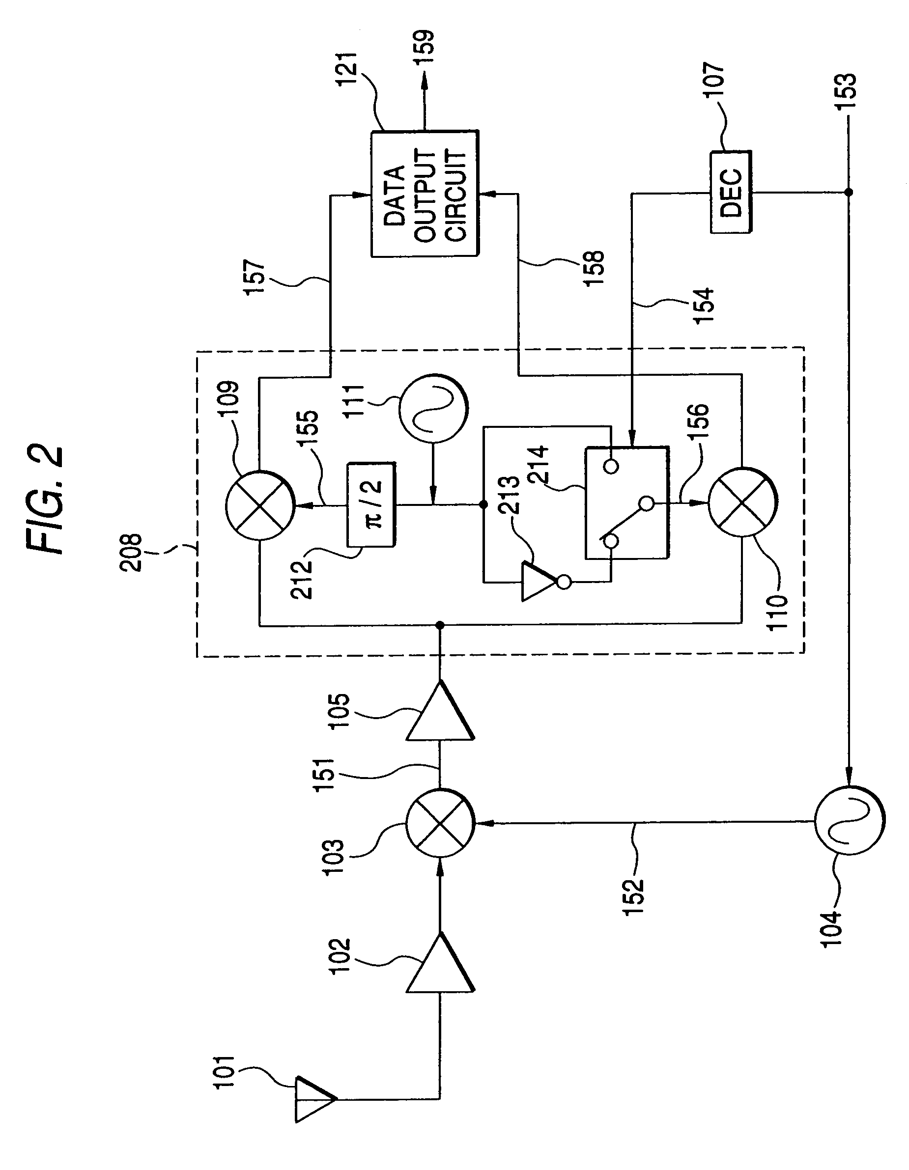
[0104]Next, FIG. 2 is a structural diagram of a multiband data communication apparatus to which either a multiband data communication apparatus or a communication method, according to a second embodiment mode of the present invention, is applied. It should be noted that the same reference numerals shown in FIG. 1 (first embodiment mode) will be employed as those for denoting the same, or similar circuit elements of this drawing, and descriptions thereof are omitted.

[0105]In the first embodiment mode, the phase of the reception local oscillation signal entered into the quadrature mixer 110 is switched so as to obtain the same reception baseband signals irrespective of the frequency relationship between the reception signal and the reception local oscillation signal. To achieve the same effect as that of the first embodiment mode, reception local oscillation signals whose phases are made different from each other are entered into both the quadrature mixers 109 and 110, and furthermore...

third embodiment

[0110]Next, FIG. 3 is a structural diagram of a multiband data communication apparatus to which either a multiband data communication apparatus or a communication method, according to a third embodiment mode of the present invention, is applied. It should be noted that the same reference numerals shown in FIG. 1 (first embodiment mode) will be employed as those for denoting the same, or similar circuit elements of this drawing, and descriptions thereof are omitted. To achieve the same effect as that of the first embodiment mode, in a quadrature demodulator 308 according to this third embodiment mode, a switch circuit 314 switches an output signal derived from a phase shifter 312 and another output signal derived from another phase shifter 313, the phase change amounts of which are different from each other.

[0111]Also, in FIG. 3, the quadrature demodulator 308 is arranged by employing quadrature mixers (first quadrature mixers) 109 and 110, a reception local oscillator (local oscilla...


PUM


Abstract

A quadrature demodulator 408′ and a quadrature modulator 908′ convert a reception intermediate frequency signal 151 into reception baseband signals 157 and 158, and also convert transmission baseband signals 657 and 658 into a transmission intermediate frequency signal 651, respectively. While local oscillation signals having frequencies suitable for the respective bands are outputted from a commonly used local oscillator 111, such a local oscillation signal obtained by shifting a phase thereof π / 2 by a phase shifter 412 is supplied to one mixer of quadrature mixers 109 and 609, and such a signal obtained by inverting, or not inverting the plurality of the local oscillation signal by an exclusive OR gate circuit 413 in response to a band switching signal 153 is supplied to the other mixer of quadrature mixers 110 and 610.

Description

BACKGROUND OF THE INVENTION[0001]The present invention generally relates to a multiband data communication apparatus, a communication method of a multiband data communication apparatus, and a storage medium for storing a program used to execute the communication method of the multiband data communication apparatus. More specifically, the present invention is directed to a multiband data communication apparatus, a communication method of a multiband data communication apparatus, and a storage medium, capable of suppressing a circuit scale to a minimum circuit scale, and further capable of preventing a deterioration in a baseband signal.[0002]As a conventional dual band data communication apparatus, or a conventional multiband data communication apparatus, one conventional data communication apparatus is represented in FIG. 12. That is, FIG. 12 is an arrangement diagram of a conventional multiband data communication apparatus. In this case, as the data communication apparatus, such a ...

Claims


Application Information

Patent Timeline
Patent Type & Authority Patents(United States)
IPC IPC(8): H04L27/22H04L27/20H03D1/22H03D3/00H03D7/16H04B1/26H04B1/30H04B1/40H04L
CPCH04B1/0082H03D7/166
Inventor NAMURA, YASUAKI
Owner PANASONIC CORP
Learn More