

Field programmable gate array (FPGA) configuration data path for module communication
a configuration data and module technology, applied in the field of programmable logic devices, can solve the problems of large fpga resources consumed by schemes, speed, resource and power penalties, and bottlenecks in the transfer of blocks between block ram columns
- Summary
- Abstract
- Description
- Claims
- Application Information
AI Technical Summary
Problems solved by technology
Method used
Image

Examples
Embodiment Construction
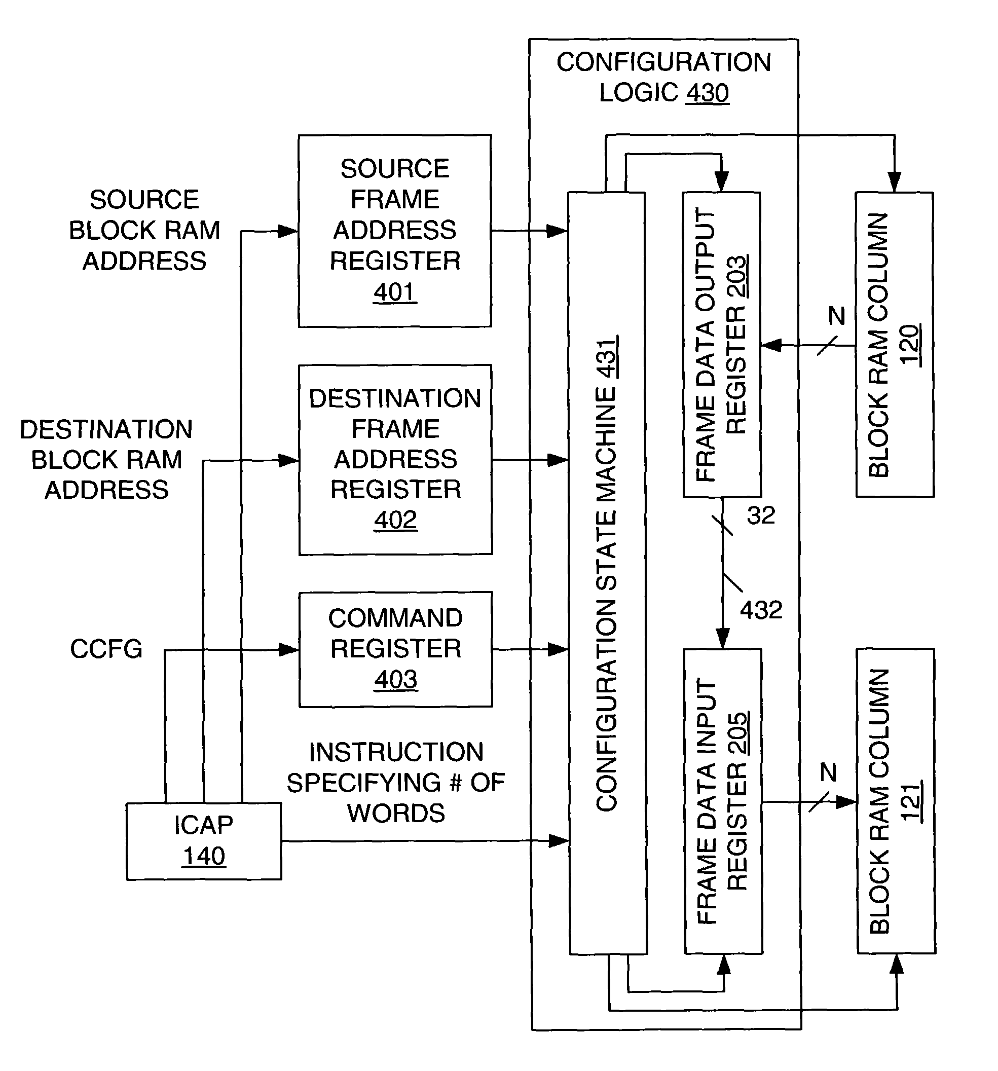
[0021]FIG. 4 is a block diagram of a data transfer system 400 of an FPGA in accordance with one embodiment of the present invention. Data transfer system 400 is located on an FPGA similar to FPGA 100 (FIG. 1). Thus, similar elements in FIGS. 1 and 4 are labeled with the same or similar reference numbers. Data transfer system 400 includes source frame address register 401, destination frame address register 402, command register 403, configuration logic 430 (which includes frame data output register 203, frame data input register 205, configuration state machine 431 and 32-bit configuration bus 432), block RAM columns 120–121 and ICAP module 140. Data transfer system 400 is capable of directly transferring data from block RAM column 120 to block RAM column 121 (or vice versa) over the 32-bit configuration bus 432. Although the present invention is described in connection with two block RAM columns 120–121, it is understood that the present invention can be applied to an FPGA having m...
PUM
 Abstract
Description
Claims
Application Information