Manufacturing method of acoustic sensor

a manufacturing method and acoustic sensor technology, applied in the field of acoustic sensors, can solve problems such as difficult size reduction

Inactive Publication Date: 2006-07-25
HOSHIDEN ELECTRONICS CO LTD
View PDF13 Cites 69 Cited by
  • Summary
  • Abstract
  • Description
  • Claims
  • Application Information

AI Technical Summary

Problems solved by technology

For this kind of electret condenser microphone, in particular, since an independent FET was used for impedance conversion, reduction of size was difficult.

Method used


Image

  • Manufacturing method of acoustic sensor
  • Manufacturing method of acoustic sensor
  • Manufacturing method of acoustic sensor

Examples


Embodiment Construction

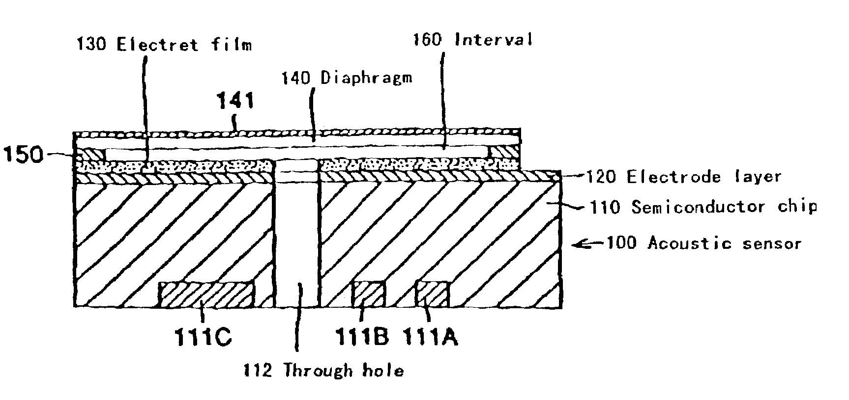
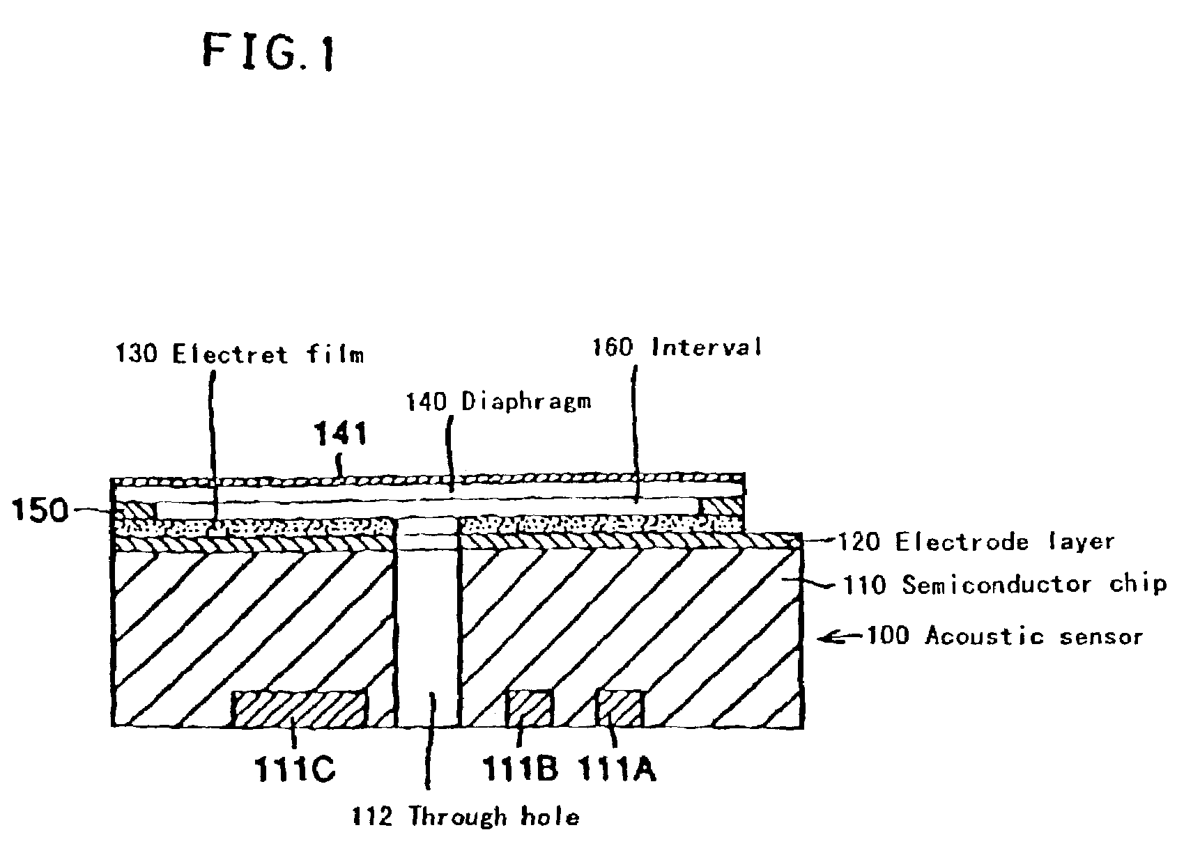
[0032]An embodiment of the invention is an acoustic sensor 100 which includes a semiconductor chip 110 forming an FET circuit 111A, a response gain control circuit 111B, an amplifying circuit 111C and others as necessary electronic circuits, and opening a through hole 112 away from the FET circuit 111A and others, an electret film 130 laminated away from the gate electrode 111a of the FET circuit 111A and the through hole 112 formed in the semiconductor chip 110, and a diaphragm 140 disposed with a spacing to this electret film 130.

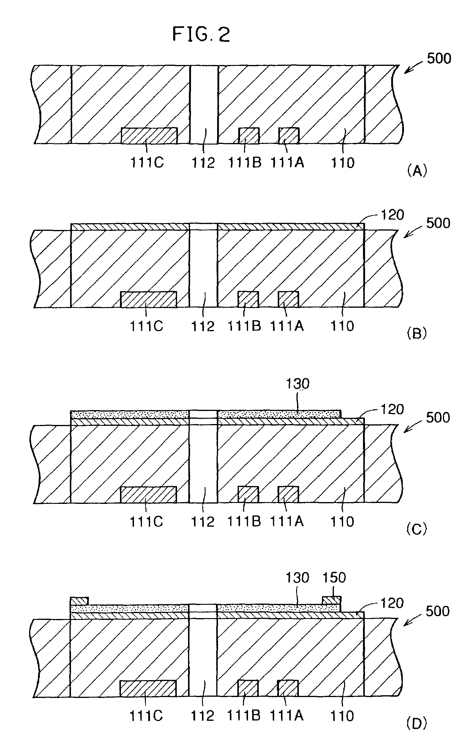
[0033]The construction of the acoustic sensor 100 is described below according to its manufacturing method.

[0034]A multiplicity of the acoustic sensors 100 are formed simultaneously on a wafer 500.

[0035]A plurality of through holes 112 are opened in the wafer 500 (see FIG. 2 (A)). The through hole 112 is opened in the center of one acoustic sensor 100 by ultrasonic processing or laser processing. The diameter of the through hole 112 is preferably 0.5 mm o...


PUM

PropertyMeasurementUnit
diameteraaaaaaaaaa
thicknessaaaaaaaaaa
thicknessaaaaaaaaaa

Abstract

The present invention relates to a semiconductor electret condenser microphone capable of being reduced in size and including an acoustic sensor 100 and a case 200 for accommodating the acoustic sensor 100, the acoustic sensor 100 has a semiconductor chip 110 forming necessary electronic circuits 111A to 111C, and opening a through hole 112 away from the electronic circuits 111A to 111C, an electrode layer 120 formed on the surface of the semiconductor chip 110 away from the through hole 112, an electret member 130 laminated away from part of the electrode layer 120 and through hole 112, and a diaphragm 140 provided with a spacing 160 to the electret member 130, in which the electrode layer 120 exposed from the electret member 130 is connected to the electrode 111a of the electronic circuit 111A through the case 200 (FIG. 6).

Description

CROSS-REFERENCES TO RELATED APPLICATIONS[0001]This application is a divisional application of U.S. application Ser. No. 09 / 145,293, filed on Sep. 2, 1998, now abandoned. The disclosure of the prior application is hereby incorporated by reference herein in its entirety.BACKGROUND OF THE INVENTION[0002]1. Field of the Invention[0003]The present invention relates to an acoustic sensor, a manufacturing method for the acoustic sensor, and a semiconductor electret condenser microphone using the acoustic sensor.[0004]2. Description of the Related Art[0005]The electret condenser microphone is widely used in mobile telephones because it is easily reduced in size. An example of an art-known electret condenser microphone is shown in FIG. 10. This electret condenser microphone includes a case 1, a diaphragm 7 provided in this case 1, an electret film 5 (formed in the case 1) disposed opposite to this diaphragm 7, and an amplifying element 9 for amplifying the change of voltage due to change of ...

Claims


Application Information

Patent Timeline
Patent Type & Authority Patents(United States)
IPC IPC(8): H04R31/00H04R19/00H04R19/01H04R19/04H04R25/00
CPCH04R19/005H04R31/00H04R19/016Y10T29/49002Y10T29/49005Y10T29/4908Y10T29/49798H04R31/006
Inventor KAWAMURA, TAKAOOHBAYASHI, YOSHIAKIYASUDA, MAMORU
Owner HOSHIDEN ELECTRONICS CO LTD
Why Eureka
Try Eureka