

Method for forming silicon dioxide film using siloxane
a technology of silicon dioxide and siloxane, applied in the direction of coating, chemical vapor deposition coating, metallic material coating process, etc., can solve the problems of poor step coverage, high deposition rate of pecvd, and limited use of cvd methods, so as to improve the deposition rate, and reduce the impurity content of the film
Inactive Publication Date: 2006-08-01
SAMSUNG ELECTRONICS CO LTD
View PDF29 Cites 228 Cited by
- Summary
- Abstract
- Description
- Claims
- Application Information
AI Technical Summary
Benefits of technology
[0015]In accordance with a preferred embodiment of the present invention, a substituted siloxane with at least two Si atoms is used as a Si source. Therefore, the silicon dioxide film formed according to the present invention provides excellent film quality due to a strong siloxane (Si—O—Si)
Problems solved by technology
PECVD provides a high deposition rate at a low temperature but poor step coverage.
For these reasons, these CVD methods have been used only in a limited manner for silicon dioxide film formation.
Recently, as semiconductor devices become highly integrated, a short channel effect caused by high temperatures in CVD methods has also been recognized as a major problem.
Therefore, low temperature silicon dioxide film formation methods are required.
In addition to the above problems, as the step-to-step height on a semiconductor substrate increases,
Method used
View moreImage
Smart ImageViewing Examples

Examples
 PUM
| Property | Measurement | Unit |
|---|---|---|
| Temperature | aaaaa | aaaaa |
| Temperature | aaaaa | aaaaa |
| Temperature | aaaaa | aaaaa |
Abstract
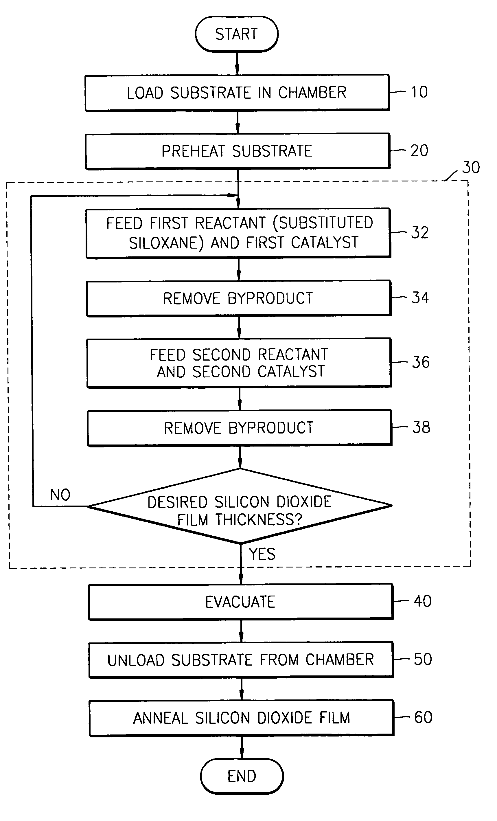
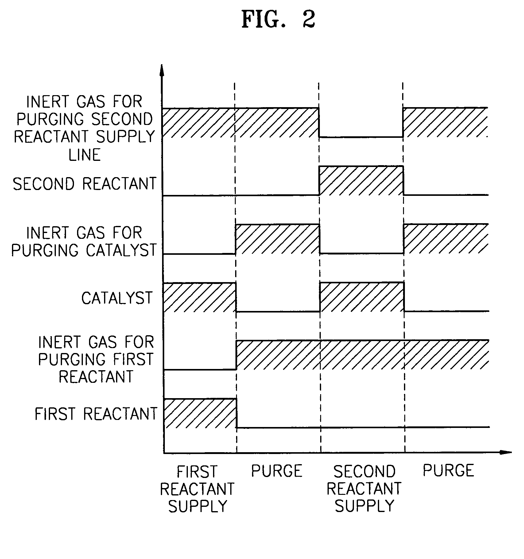
A method is provided for forming a silicon dioxide film using atomic layer deposition (ALD), wherein a halogen- or NCO-substituted siloxane is used as a Si source. The method includes feeding a substituted siloxane as a first reactant onto a substrate to form a chemisorbed layer of the first reactant, and thereafter feeding a compound consisting of oxygen and hydrogen as a second reactant onto the chemisorbed layer to form the desired silicon dioxide film.
Description
[0001]This application is a continuation-in-part application of U.S. patent application Ser. No. 10 / 459,943, filed Jun. 12, 2003, the disclosure of which is incorporated herein in its entirety by reference.[0002]This application claims the priority of Korean Patent Application No. 2003-12324, filed on Feb. 27, 2003 and No. 2004-7104 filed on Feb. 4, 2004, in the Korean Intellectual Property Office, the disclosure of which is incorporated herein in its entirety by reference.BACKGROUND OF THE INVENTION[0003]1. Field of the Invention[0004]The present invention relates to a method for forming a thin film on a substrate, and more particularly to a method for forming a silicon dioxide film using atomic layer deposition (ALD).[0005]2. Description of the Related Art[0006]As the sizes of microelectronics devices continue to become smaller, the qualities of silicon dioxide films that are used as gate oxide films and dielectric films of electric field effect transistors in semiconductor device...
Claims
Login to View More Application Information
Patent Timeline
 IPC IPC(8): H01L21/31C23C16/40C23C16/44C23C16/455H01L21/312H01L21/316
CPCC23C16/402C23C16/45534H01L21/02164H01L21/02216H01L21/31612H01L21/0228H01L21/02337H01L21/0234H01L21/3122H01L21/02277
InventorPARK, JAE-EUNCHU, KANG-SOOLEE, JOO-WONYANG, JONG-HO
OwnerSAMSUNG ELECTRONICS CO LTD