Trench type buried on-chip precision programmable resistor

a precision programmable resistor and on-chip technology, applied in the field of electromechanical devices, can solve the problems of temperature resistance variation and space occupancy, and achieve the effect of precise resistance value, small surface area of space, and low nois

Inactive Publication Date: 2006-08-01
GLOBALFOUNDRIES INC
View PDF11 Cites 10 Cited by
  • Summary
  • Abstract
  • Description
  • Claims
  • Application Information

AI Technical Summary

Benefits of technology

[0012]In each of the first and second embodiments, each column and row of the resistor array is separated by isolation (such as trench isolation or STI) or local oxidation of silicon (LOCOS) to minimize noise. The whole substrate serves as a good heat sink for thermal dissipation. The whole resistor structure is ultra-compact, taking up a small surface area of space. Further, utilizing the trench array concept of the invention, blocks of arrays may be connected through fuses that may be blown to form a resultant resistor structure of a very precise resistance value.

Problems solved by technology

For polysilicon resistors which are placed on the surface of the Si substrate, precision control of resistance (control of doping level), doping uniformity, resistance variation due to temperature, and space occupancy are also of serious concerns.

Method used


Image

  • Trench type buried on-chip precision programmable resistor
  • Trench type buried on-chip precision programmable resistor
  • Trench type buried on-chip precision programmable resistor

Examples


first embodiment

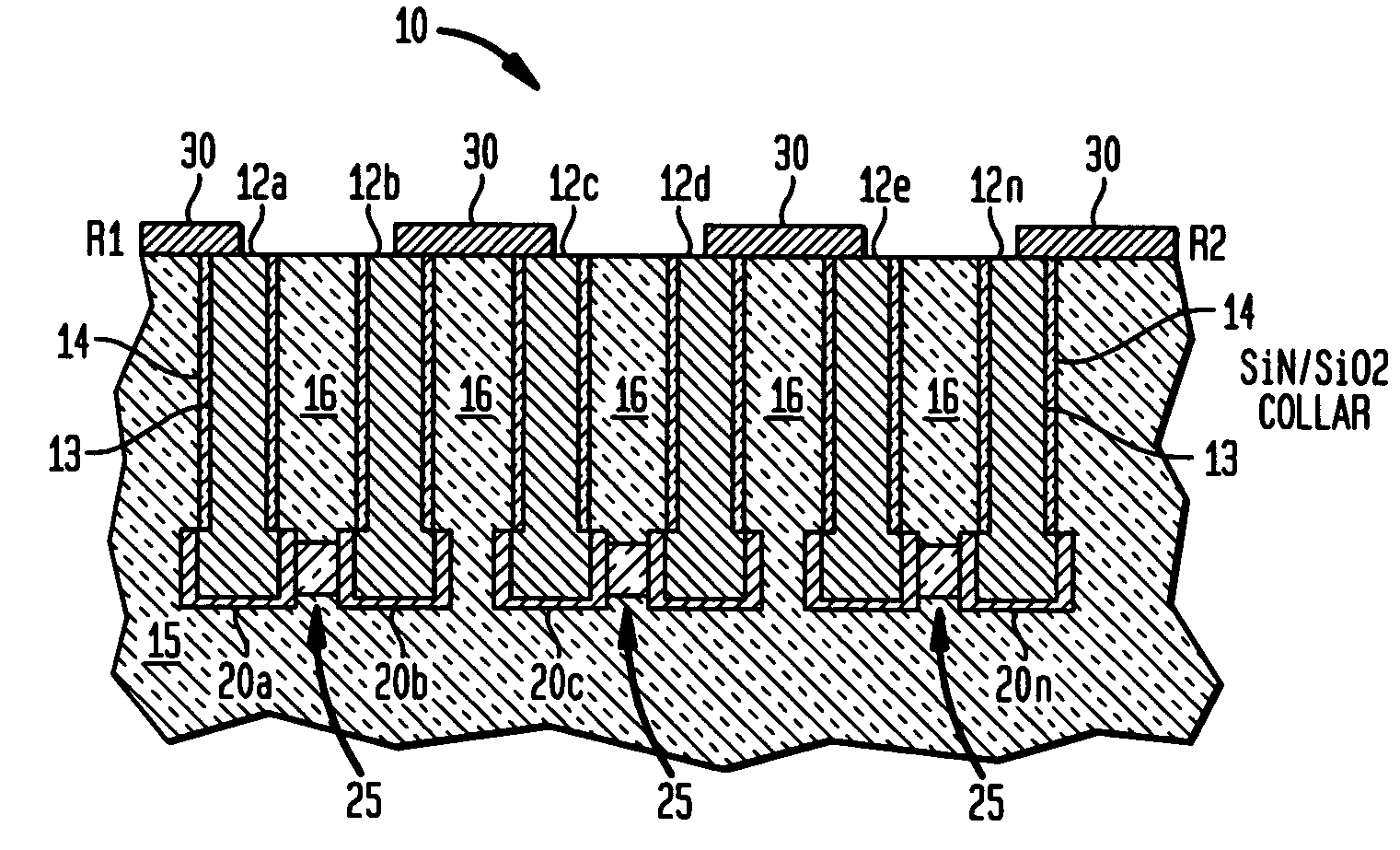
[0021]FIG. 1 illustrates a cross-sectional view of a trench type buried resistor 10 according to the invention. As shown in FIG. 1, the trench buried type resistor includes a series of trenches 12a, 12b, . . . , 12n formed in a substrate 15, aligned, for example, in a row, with each trench separated by a dielectric region 16, e.g., an oxide. Each trench 12a, 12b, . . . , 12n is filled with a conductor material 13 such as Tantalum Nitride (TaN) or Polysilicon, and each trench includes a buried plate bottom connective portion 20a, 20b, . . . , 20n. As shown in FIG. 1, between alternating adjacent first trenches, e.g., trenches 12a, 12b and 12c, 12d, etc., there are formed ion implantation bands 25 comprising ion implanted doped substrate material that connect these adjacent trenches in alternating fashion. Likewise, between alternating adjacent second trenches 12b, 12c and 12d, 12e etc., there are formed top surface resistive connective portions 30 that connect these adjacent trenches...

second embodiment

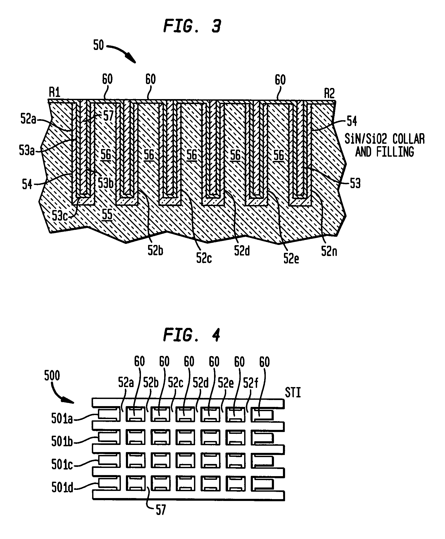
[0026]FIG. 3 illustrates a cross-sectional view of a trench type buried resistor 50 according to the invention. As shown in FIG. 3, the trench buried type resistor includes a series of trenches 52a, 52b, . . . , 52n formed in a substrate 55, aligned, for example, in a row, with each trench separated by a dielectric region 56, e.g., an oxide. Each trench 52a, 52b, . . . , 52n includes a buried thin layer 53 of conductive material such as TaN or Polysilicon, shaped in conformance with the shape of the trench and having side 53a,b and bottom 53c portions. This thin conductive material layer may range between 50 Å and 500 Å in thickness depending upon the desired resistance, e.g., as dictated by circuit requirements. Between each trench 52a, 52b, . . . , 52n there is formed a top surface resistive connector portion 60 that connects each buried thin layer 53 (conductive layer sidewalls 53a,b) of a trench with the buried thin conductive layer 53 of an adjacent trench, thus forming a serie...


PUM


Abstract

An on-chip, ultra-compact, and programmable semiconductor resistor device and device structure and a method of fabrication. Each semiconductor resistor device structure is formed of one or more conductively connected buried trench type resistor elements exhibiting a precise resistor value. At least two semiconductor resistor device structures may be connected in series or in parallel configuration through the intermediary of one or more fuse devices that may be blown to achieve a desired total resistance value.

Description

BACKGROUND OF INVENTION[0001]1. Field of the Invention[0002]The present invention relates generally to electronic devices and specifically, is directed to the manufacture of compact, precision semiconductor on-chip resistors and precision resistor array devices having improved properties.[0003]2. Description of the Prior Art[0004]Conventional on-chip resistors made of TaN or polysilicon are either placed within the multi-level Back End of Line (BEOL) interconnect layers or placed on the surface of a Si substrate. For TaN precision on-chip resistors which are placed within the metal levels, heat dissipation, thermally induced electromigration (EM) of neighboring interconnect wires, and the space occupancy are all of some concern. For polysilicon resistors which are placed on the surface of the Si substrate, precision control of resistance (control of doping level), doping uniformity, resistance variation due to temperature, and space occupancy are also of serious concerns. Therefore,...

Claims


Application Information

Patent Timeline
Patent Type & Authority Patents(United States)
IPC IPC(8): H01L29/00H01L21/20H01L27/10
CPCH01L28/20H01L27/101
Inventor AITKEN, JOHN M.CHEN, FENSULLIVAN, TIMOTHY D.
Owner GLOBALFOUNDRIES INC
Why Eureka
Try Eureka