Thin-film transistor array substrate

a transistor array and thin film technology, applied in non-linear optics, instruments, optics, etc., can solve the problems of space utilization and power consumption of cathode ray tubes, increase the fabrication cost, etc., and achieve the effect of reducing the fabrication cos

Inactive Publication Date: 2006-08-01
AU OPTRONICS CORP
View PDF5 Cites 38 Cited by
  • Summary
  • Abstract
  • Description
  • Claims
  • Application Information

AI Technical Summary

Benefits of technology

[0009]The present invention provides a thin-film transistor array substrate used in transreflective liquid crystal display. Each of the sub-pixels has a pixel electrode connected to different thin-film transistor to save the step for forming a molybdenum layer. Therefore, the fabrication cost is reduced.

Problems solved by technology

However, issues of space utilization and power consumption exist in cathode ray tubes.
However, in the conventional thin-film transistor array substrate, the molybdenum layer, though improving the corrosion problem caused by electrochemical reaction, increases the fabrication cost.

Method used


Image

  • Thin-film transistor array substrate
  • Thin-film transistor array substrate
  • Thin-film transistor array substrate

Examples


first embodiment

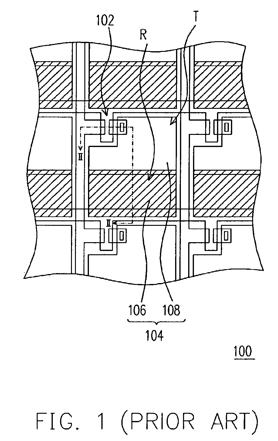
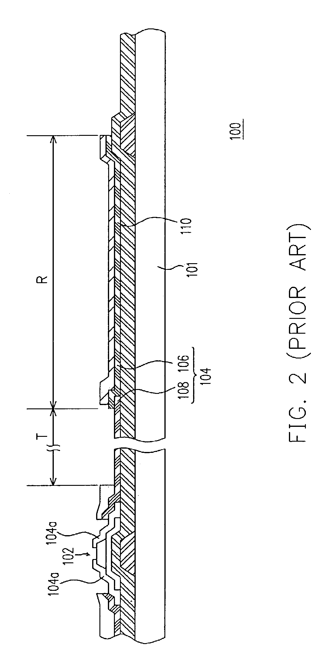
[0018]Referring to FIG. 3, in the present invention, a thin-film transistor array substrate 200 of a transreflective liquid crystal display comprises a substrate (not shown), a plurality of pixels 204, a plurality of scan lines 210 and a plurality of data lines 220. Each of the pixels 204 is located between two neighboring scan lines 210 and two neighboring data lines 220. Each pixel 204 has a plurality of sub-pixels.

[0019]In this embodiment, each pixel 204 has a transparent sub-pixel 204′ and a reflective sub-pixel 204″. Each transparent sub-pixel 204′ defines a transparent region T, while each reflective sub-pixel 204″ defines a reflective region R. Each transparent sub-pixel 204′ includes a transparent pixel electrode 208 and a first thin-film transistor 202a, while each reflective sub-pixel 204″ has a reflective pixel electrode 206 and a second thin-film transistor 202b. The reflective pixel electrode 206 is made of a material with high reflectivity such as aluminum, silver, tan...

second embodiment

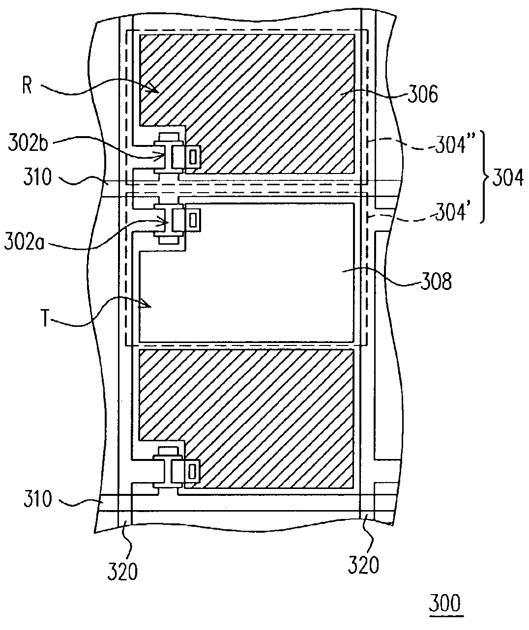
[0022]FIG. 4 shows a top view of a thin-film transistor array substrate 300 of a transreflective liquid crystal display in the present invention. The thin-film transistor array substrate 300 comprises a substrate (not shown), a plurality of pixels 304, a plurality of scan lines 310 and a plurality of data lines 320. The pixels 304 are located on the substrate between two neighboring data lines 320. Each of the pixels 304 has a transparent sub-pixel 304′ and a reflective sub-pixel 304″. The transparent sub-pixel 304′ defines a transparent region T, while the reflective sub-pixel 304″ defines a reflective region R. The transparent sub-pixel 304′ comprises a transparent pixel electrode 308 and a first thin-film transistor 302a, and the reflective sub-pixel 304″ comprises a reflective pixel electrode 306 and a second thin-film transistor 302b.

[0023]In this embodiment, the first thin-film transistor 302a and the second thin-film transistors 302b are disposed at opposing sides of the tra...

third embodiment

[0024]FIG. 5 shows a top view of a thin-film transistor array substrate 400 of a transreflective liquid crystal display in the present invention. The thin-film transistor array substrate 400 comprises a substrate (not shown), a plurality of pixels 404, a plurality of scan lines 410 and a plurality of data lines 420. The pixels 404 are located on the substrate between two neighboring data lines 420. Each of the pixels 404 has a transparent sub-pixel 404′ and a reflective sub-pixel 404″. The transparent sub-pixels 404′ define a transparent region T, while the reflective sub-pixels 404″ define a reflective region R. Each transparent sub-pixel 404′ comprises a transparent pixel electrode 408 and a first thin-film transistor 402a, and each reflective sub-pixel 404″ comprises a reflective pixel electrode 406 and a second thin-film transistor 402b.

[0025]In this embodiment, the first thin-film transistors 402a and the second thin-film transistors 402b are disposed at different sides of the...


PUM

PropertyMeasurementUnit
transparentaaaaaaaaaa
corrosionaaaaaaaaaa
reflectivityaaaaaaaaaa

Abstract

A thin-film transistor array substrate, used in a transflective liquid crystal display. The thin-film transistor array substrate has a substrate, a plurality of pixels, a plurality of scan lines and a plurality of data lines. Each of the pixels has a transparent sub-pixel and a reflective sub-pixel, while the transparent sub-pixel further has a transparent electrode and a first thin-film transistor, and the reflective sub-pixel has a reflective pixel electrode and a second thin-film transistor. The pixel electrode of each sub-pixel is thus electrically connected to a different thin-film transistor. The step of forming a molybdenum layer is thus not required, saving fabrication cost.

Description

CROSS REFERENCE TO RELATED APPLICATIONS[0001]This application claims the priority benefit of Taiwan application serial no. 91114696, filed Jul. 03, 2002.BACKGROUND OF INVENTION[0002]1. Filed of the Invention[0003]The invention relates in general to a thin-film transistor array substrate typically used in a transflective liquid crystal display, and more particularly, to a thin-film transistor array substrate of which the pixel electrodes of the transparent sub-pixels and reflective sub-pixels are electrically connected to different transistors.[0004]2. Related Art of the Invention[0005]The advancement of multimedia basically results from the progress of semiconductor device or display apparatus design. Conventional display apparatus such as the cathode ray tube (CRT) have dominated the market for decades due to its excellent display quality and economics. However, issues of space utilization and power consumption exist in cathode ray tubes. Therefore, the light, thin, short and small...

Claims


Application Information

Patent Timeline
Patent Type & Authority Patents(United States)
IPC IPC(8): G02F1/1368G02F1/1343G02F1/1335G02F1/1362
CPCG02F1/133555G02F1/1368G02F1/13624G02F2001/134345G02F1/134345
Inventor LUO, FANG-CHEN
Owner AU OPTRONICS CORP
Why Eureka
Try Eureka