

Electronic circuit design method, simulation apparatus and computer-readable storage medium
a technology of electronic circuit and simulation apparatus, applied in computer aided design, program control, instruments, etc., can solve the problems of time-consuming and laborious design of electronic circuit, generating reflection noise, and not being able to secure all
- Summary
- Abstract
- Description
- Claims
- Application Information
AI Technical Summary
Benefits of technology
Problems solved by technology
Method used
Image

Examples
first embodiment
[0042]FIG. 4 is a diagram showing a wiring pair which is to be subjected to a design modification in a first embodiment. The wiring pair is formed by an aggressor net 1 which becomes a crosstalk noise generating source, and a victim net 2. Crosstalk noise is generated in the victim net 2, because the aggressor net 1 is adjacent to the victim net 2 at an adjacent wiring portion 3.
[0043]The crosstalk noise is generated in the victim net 2, because the aggressor net 1 is too close to the victim net 2 at the adjacent wiring portion 3. Hence, the design modification is automatically made, so as to automatically provide a spacing 4 between the aggressor net 1 and the victim net 2 at the adjacent wiring portion 3, as shown in FIG. 5. FIG. 5 is a diagram for explaining the design modification which automatically provides the spacing 4 between the aggressor net 1 and the victim net 2 at the adjacent wiring portion 3.
[0044]FIG. 6 is a diagram showing a check result list 20 which is output by ...
second embodiment
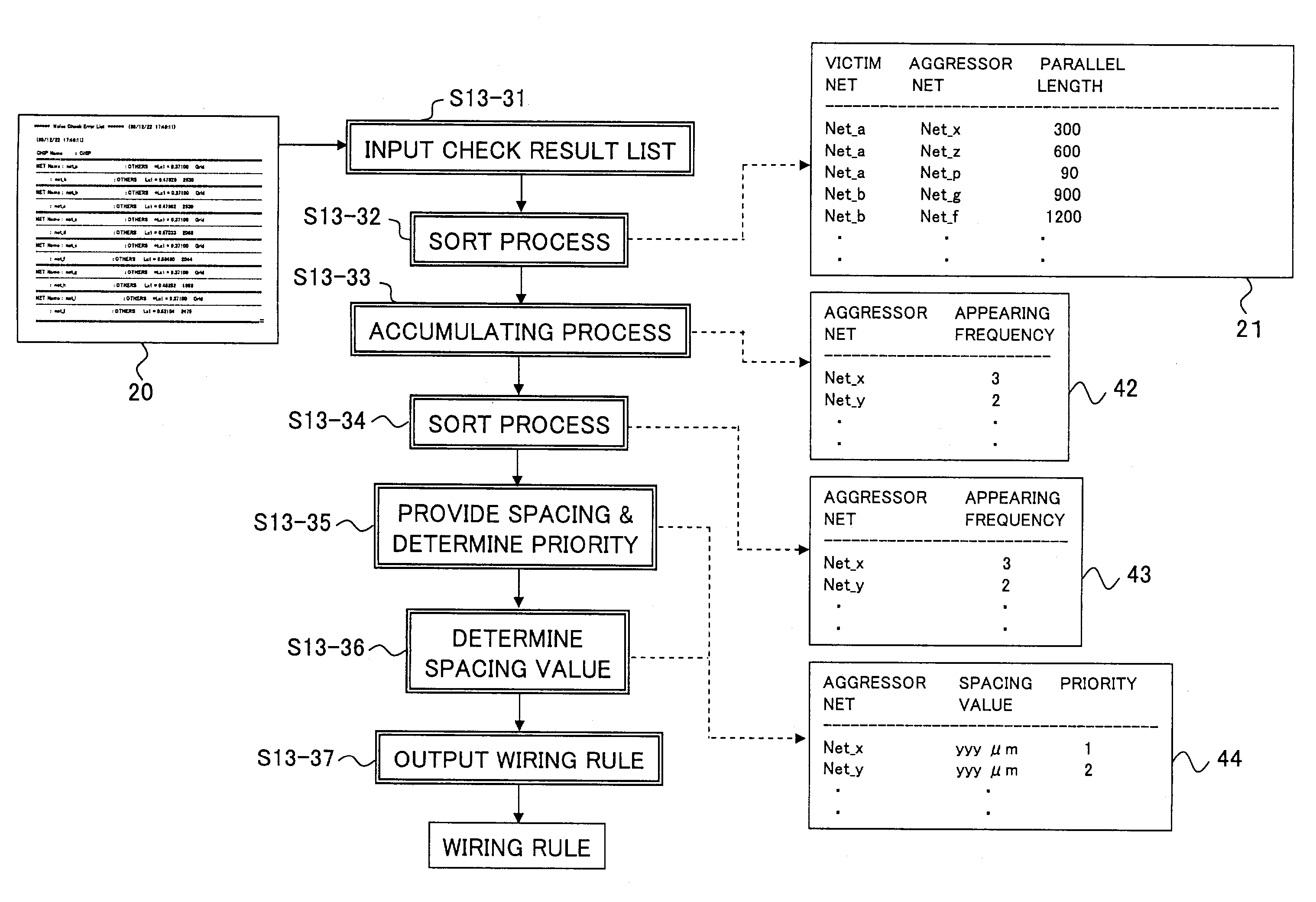
[0050]FIG. 8 is a flow chart for explaining an important part of the operation of a second embodiment. The process shown in FIG. 8 corresponds to the step S13 shown in FIG. 3.
[0051]In FIG. 8, a step S13-11 inputs the check result list 20 shown in FIG. 6, and a step S13-12 generates a list 21 on the right side of FIG. 8 by carrying out a sort process. The list 21 includes the victim net, the aggressor net, and the length of parallel wirings between the aggressor net and the aggressor net at the adjacent wiring portion. A step S13-13 carries out an accumulating process to obtain the length of parallel wirings with respect to each victim net and to generate a list 22 shown on the right side of FIG. 8. A step S13-14 carries out a sort process with respect to the list 22, and generates a list 23 shown on the right side of FIG. 8. For example, the contents of the list 22 are sorted in an order starting from the largest length of parallel wirings. In this sort process, the spacing is secur...
third embodiment
[0054]FIG. 9 is a flow chart for explaining an important part of the operation of a third embodiment. The process shown in FIG. 9 corresponds to the step S13 shown in FIG. 3.
[0055]In FIG. 9, a step S13-21 inputs the check result list 20 shown in FIG. 6, and a step S13-22 generates a list 21 on the right side of FIG. 9 by carrying out a sort process. The list 21 includes the victim net, the aggressor net, and the length of parallel wirings between the aggressor net and the aggressor net at the adjacent wiring portion. A step S13-23 carries out an accumulating process to obtain the appearing frequency of each victim net in the list 21 and to generate a list 32 shown on the right side of FIG. 9. A step S13-24 carries out a sort process with respect to the list 32, and generates a list 33 shown on the right side of FIG. 9. For example, the contents of the list 32 are sorted in an order starting from the highest appearing frequency. In this sort process, the spacing is secured with respe...
PUM
 Abstract
Description
Claims
Application Information