Apparatus and methods for minimizing arcing in a plasma processing chamber

Active Publication Date: 2006-08-08
LAM RES CORP
View PDF21 Cites 175 Cited by
  • Summary
  • Abstract
  • Description
  • Claims
  • Application Information

AI Technical Summary

Benefits of technology

[0017]The invention relates, in one embodiment, to a plasma processing chamber for processing a substrate to form electronic components thereon. The plasma processing chamber includes a plasma-facing component having a plasma-facing surface oriented toward a plasma in the plasma processing chamber during processing of the substrate, the plasma-facing component being electrically isolated from a ground terminal. The plasma processing chamber further includes a grounding arrangement coupled to the plasma-facing component,

Problems solved by technology

Such leakage may cause premature corrosion and/or result in the inappropriate deposition of unwanted materials on certain chamber parts.
Although aluminum is relatively inexpensive and easy to fabricate, it suffers from chemical incompatibility with certain etch processes, such as those involved in etching aluminum layers on the substrate surface.
Even with an anodized coating or some other coatings, the risk of contamination due to the unwanted presence of aluminum-containing particles in the chamber makes aluminum unacceptable in certain applications.
Such aluminum-containing particles may cause unwanted deposition of contaminants on the substrate being processed, or may be incorporated into the polymer deposition along the chamber sidewalls, rendering the chamber cleaning task more difficult and more time-consuming to perform.
Some materials may have the right chemical and electrical properties but may, for example, be very difficult and/or expensive to fabricate and/or to produce with the requisite degree of purity.
Thus, no material is perfect for every application, and one that is chemically compatible and results in low contamination often suffers from other deficiencies, such as undesirable electrical properties.
Arcing is a serious problem, as it detrimentally degrades

Method used


Image

  • Apparatus and methods for minimizing arcing in a plasma processing chamber
  • Apparatus and methods for minimizing arcing in a plasma processing chamber
  • Apparatus and methods for minimizing arcing in a plasma processing chamber

Examples


Example

[0031]The present invention will now be described in detail with reference to a few preferred embodiments thereof as illustrated in the accompanying drawings. In the following description, numerous specific details are set forth in order to provide a thorough understanding of the present invention. It will be apparent, however, to one skilled in the art, that the present invention may be practiced without some or all of these specific details. In other instances, well known process steps and / or structures have not been described in detail in order to not unnecessarily obscure the present invention.

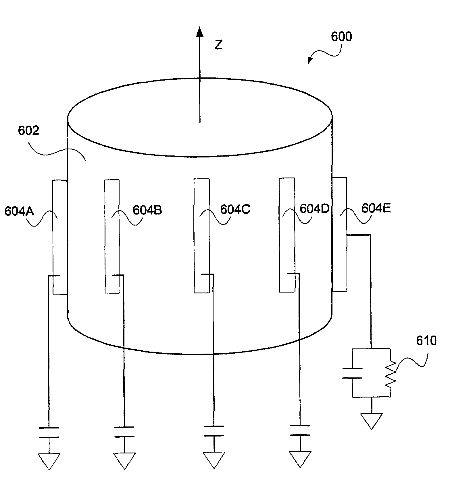
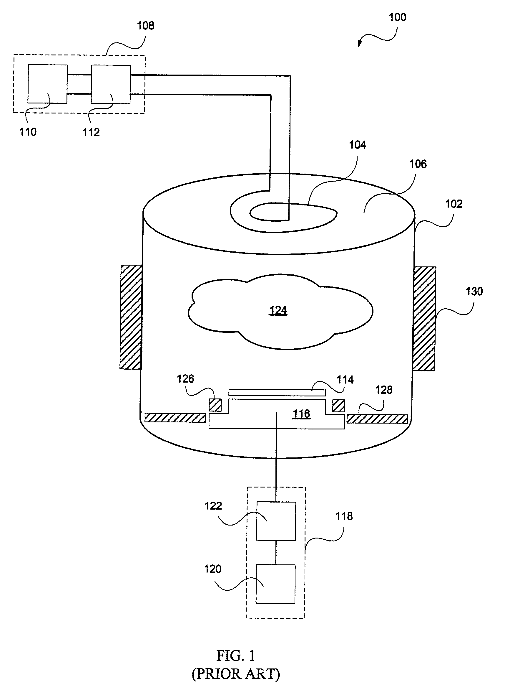
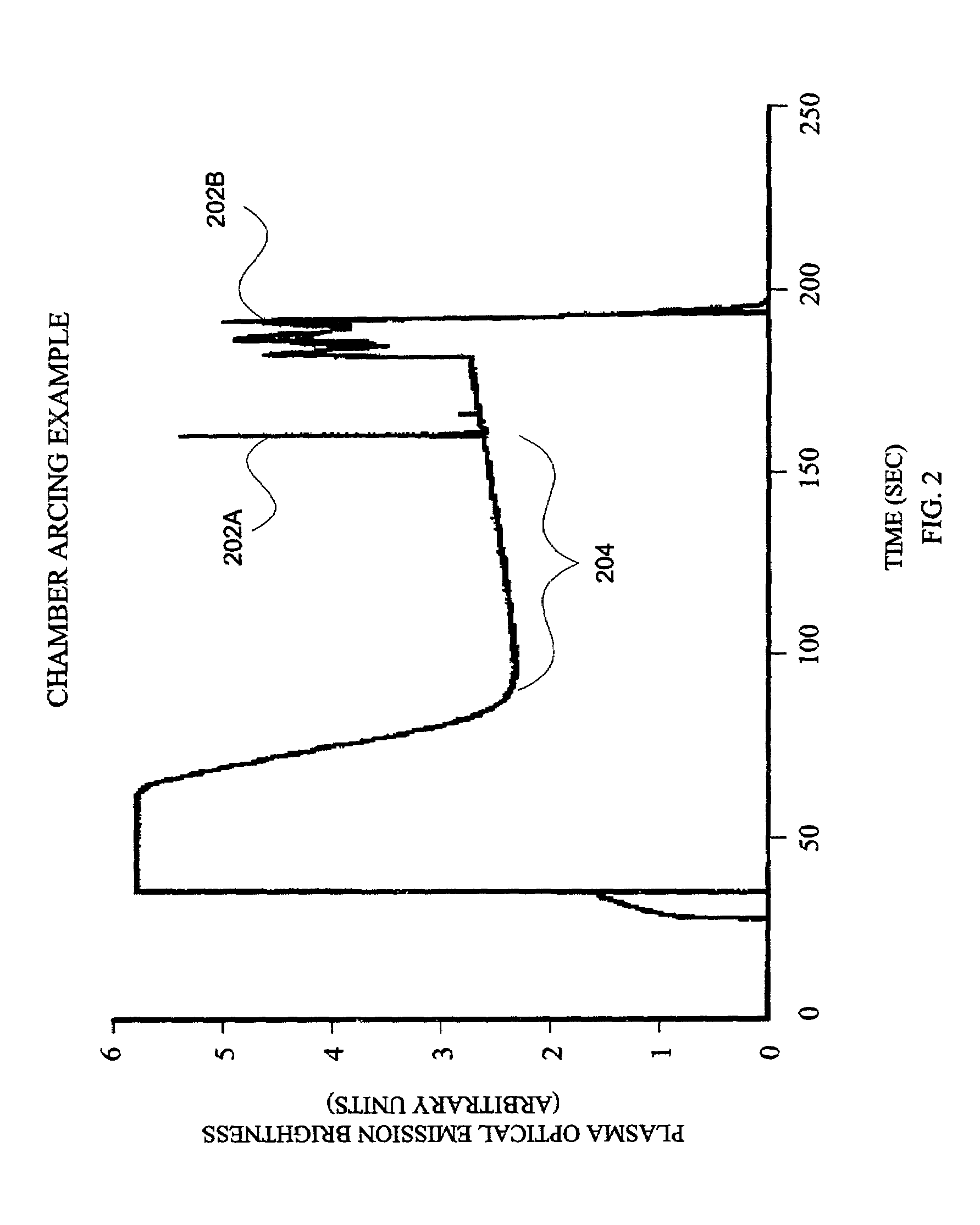
[0032]The invention relates, in one embodiment, to an arc-eliminating (AE) arrangement for eliminating arcing between a plasma-facing component and the plasma in a plasma processing chamber. While not wishing to be bound by theory, it is believed that arcing occurs because a sufficiently high DC potential is allowed to build up across a dielectric layer, such as the polymer layer deposited...


PUM

PropertyMeasurementUnit
Electrical resistanceaaaaaaaaaa
Plasma poweraaaaaaaaaa

Abstract

A plasma processing chamber for processing a substrate to form electronic components thereon is disclosed. The plasma processing chamber includes a plasma-facing component having a plasma-facing surface oriented toward a plasma in the plasma processing chamber during processing of the substrate, the plasma-facing component being electrically isolated from a ground terminal. The plasma processing chamber further includes a grounding arrangement coupled to the plasma-facing component, the grounding arrangement including a first resistance circuit disposed in a first current path between the plasma-facing component and the ground terminal. The grounding arrangement further includes a RF filter arrangement disposed in at least one other current path between the plasma-facing component and the ground terminal, wherein a resistance value of the first resistance circuit is selected to substantially eliminate arcing between the plasma and the plasma-facing component during the processing of the substrate.

Description

BACKGROUND OF THE INVENTION[0001]The present invention relates to apparatus and methods for processing substrates, such as semiconductor substrates for use in IC fabrication or glass panels for use in flat panel display fabrication. More particularly, the present invention relates to improved methods and apparatus for minimizing, during processing, arcing between a plasma-facing component associated with a plasma processing chamber and the plasma present therein and / or with another plasma-facing component.[0002]Plasma processing systems have been around for some time. Over the years, plasma processing systems utilizing inductively coupled plasma sources, electron cyclotron resonance (ECR) sources, capacitive sources, and the like, have been introduced and employed to various degrees to process semiconductor substrates and glass panels.[0003]During processing, multiple deposition and / or etching steps are typically employed. During deposition, materials are deposited onto a substrate ...

Claims


Application Information

Patent Timeline
IPC IPC(8): H01L21/00C23C16/00H05H1/46C23C16/50H01J37/32H01L21/205H01L21/306H01L21/3065H05H1/00
CPCH01J37/32623H01J37/32477H01L21/205H01L21/3065
Inventor HOWALD, ARTHUR M.KUTHI, ANDRASBAILEY, III, ANDREW D.BERNEY, BUTCH
Owner LAM RES CORP
Why Eureka
Try Eureka