AD conversion method, AD converter, semiconductor device for detecting distribution of physical quantities, and electronic apparatus

a technology of ad conversion and ad converter, which is applied in the field of analogtodigital (ad) conversion methods and ad converters, can solve the problems of insufficient processing speed, longer total period of ad conversion, and problematic schedule in terms of processing speed

Active Publication Date: 2006-08-08
SONY CORP
View PDF5 Cites 98 Cited by
  • Summary
  • Abstract
  • Description
  • Claims
  • Application Information

AI Technical Summary

Problems solved by technology

Thus, the scheme is problematic in terms of processing speed.
Thus, the total period of AD conversion becomes longer, i.e., the processing speed is not sufficient (hereinafter referred to as a first problem).
This could increase noise or power consumption (hereinafter referred to as aa fourth problem).
Furthermore, in order to hold count values of the first and second counting operations at different locations of the data storage unit 255, 2n signal lines for transmitting the results of the first and second counting operations are needed, which causes an increase in the amount of current (hereinafter referred to as a fifth problem).
This could increase noise or power consumption for transferring data (hereinafter referred to as a sixth problem).
This increases circuitry scale and circuit area, and also increases noise, consumption current, or power consumption.
Similarly to the third problem, two memories are needed for this purpose, causing an increase in circuit area (hereinafter referred to as a seventh problem).
However, lines for inputting the count clock CK0 and n count outputs from the counters to the latches are needed, so that the fourth problem is not overcome.
However, handing of a reset component and a signal component is not described, so that the third, fifth, sixth, and seventh problems are not necessarily overcome.
Thus, the third to fifth and seventh problems cannot be avoided.

Method used


Image

  • AD conversion method, AD converter, semiconductor device for detecting distribution of physical quantities, and electronic apparatus
  • AD conversion method, AD converter, semiconductor device for detecting distribution of physical quantities, and electronic apparatus
  • AD conversion method, AD converter, semiconductor device for detecting distribution of physical quantities, and electronic apparatus

Examples


first embodiment

of the Operation of the Solid-State Imaging Device

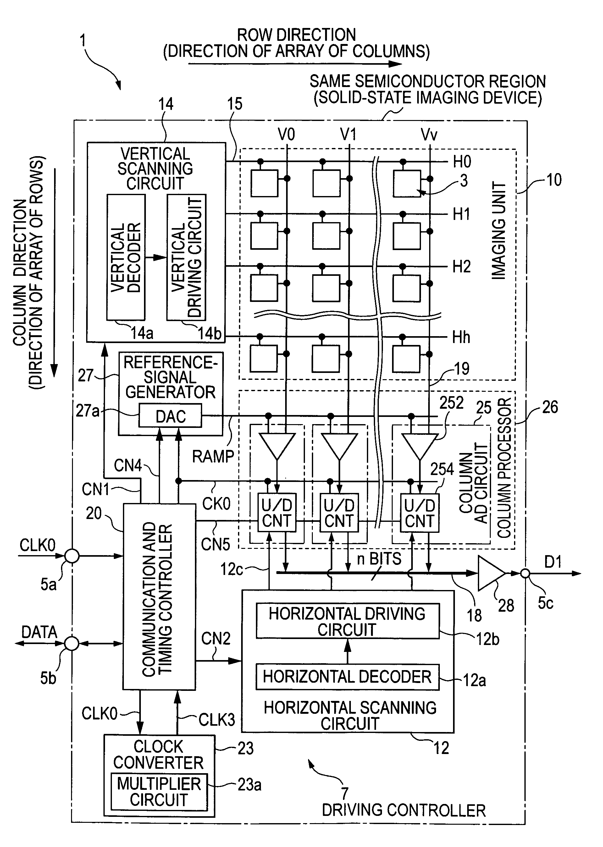
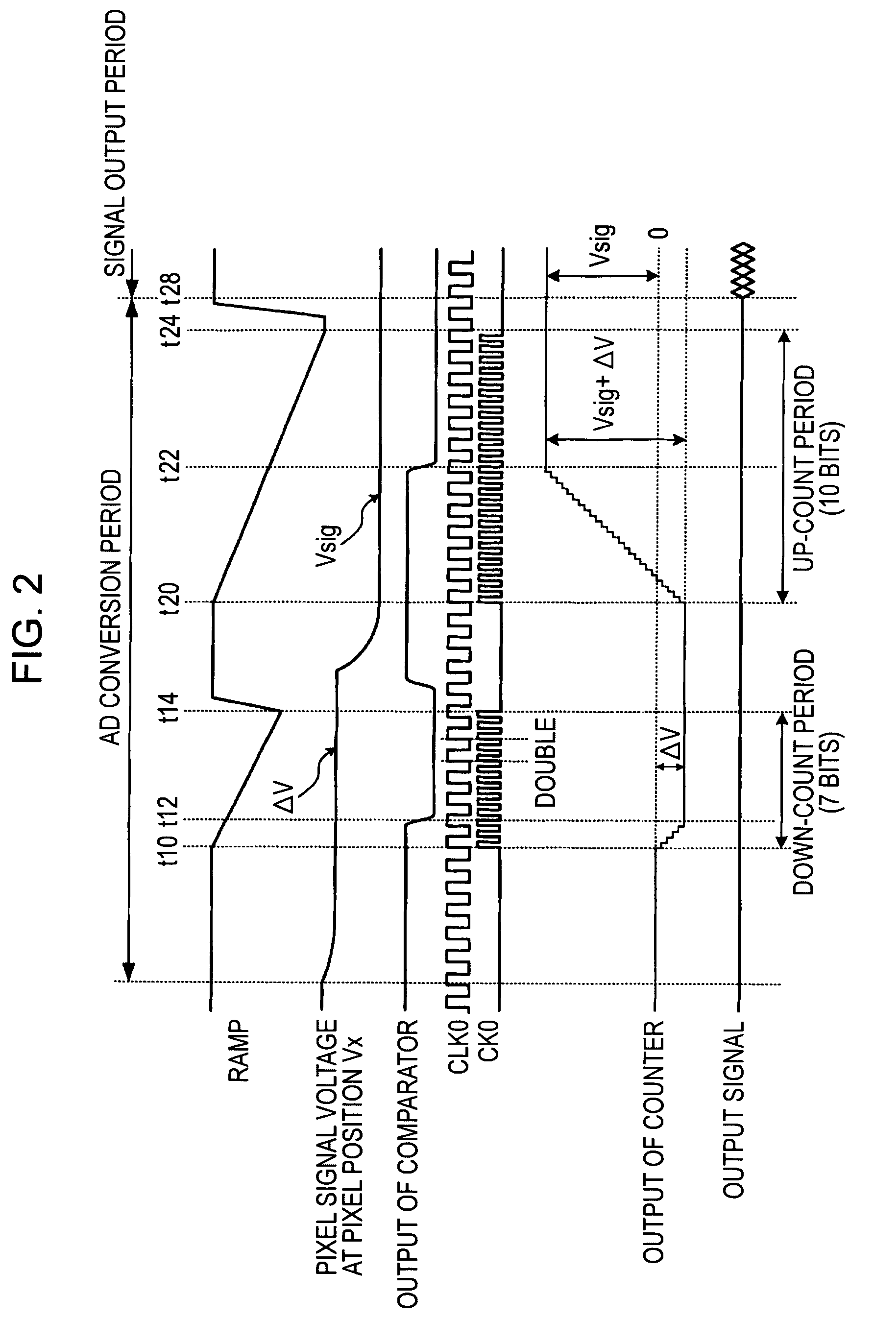
[0143]FIG. 2 is a diagram for explaining an operation of the column AD circuits 25 in the solid-state imaging device 1 according to the first embodiment shown in FIG. 1. As a mechanism for converting analog pixel signals sensed by the unit pixels 3 of the pixel unit 10 into digital signals, for example, a point where the ramp-waveform reference signal RAMP that decreases at a specific gradient matches the voltage of a reference component or signal component in pixel signals from the unit pixels 3. Then, counting is performed based on a count clock between the time when the reference signal RAMP used for comparison is generated and the time when the signal corresponding to a reference component or signal component in pixel signals matches the reference signal, whereby a count value corresponding to the magnitude of the reference component or signal component is obtained.

[0144]In a pixel signal output from the vertical signal line 19, ...

second embodiment

of the Operation of Solid-State Imaging Device

[0194]FIG. 4 is a timing chart for explaining the operation of the column AD circuits 25 in the solid-state imaging device 1 according to the second embodiment shown in FIG. 3. AD conversion in the column AD circuits 25 is performed in the same manner as in the first embodiment, so that detailed description thereof will be omitted.

[0195]In the second embodiment, the data storage units 256 are added to the construction of the first embodiment. The basic operations including AD conversion are the same as those in the first embodiment. However, before the operation of the counter 254 (t30), based on a memory transfer instruction pulse CN8 from the communication and timing controller 20, the results of counting associated with a previous row Hx−1 is transferred to the data storage units 256.

[0196]According to the first embodiment, it is possible to output pixel data to the outside of the column processor 26 only after the second reading oper...

third embodiment

of the Construction of Solid-State Imaging Device

[0199]FIG. 5 is a schematic diagram showing the construction of a CMOS solid-state imaging device (CMOS image sensor) according to a third embodiment of the present invention. FIGS. 6A to 6D are timing charts for explaining an example of data output method in the third embodiment.

[0200]A solid-state imaging device 1 according to the third embodiment differs from the solid-state imaging device 1 according to the first embodiment in that parallel data output from the column processor 26 is converted into serial data and the serial data is output to the outside of the device as video data D1. By serializing the data for output, high-speed output is allowed with a number of terminals smaller than the number of bits of digital data obtained by AD conversion. Although the third embodiment is described as a modification to the first embodiment, a similar modification to the second embodiment is also possible.

[0201]The output circuit 28 buffe...


PUM


Abstract

In a solid-state imaging device including an analog-to-digital converter, a clock converter that generates a high-speed clock that is faster than a master clock is provided. A voltage comparator compares a pixel signal input from a vertical signal line for each row control line with a reference voltage, generating pulses having magnitudes corresponding to a reset component or a signal component in a temporal direction. A counter counts the width of pulse signals until completion of the comparison in the voltage comparator based on a clock that is generated based on the high-speed clock, holding a count value at a time of completion of the comparison. A communication and timing controller exercises control so that the voltage comparator performs comparison for the reset component and the counter performs down-counting in a first processing iteration and so that the voltage comparator performs comparison for the signal component and the counter performs up-counting in a second processing iteration.

Description

RELATED APPLICATION DATA[0001]The present application claims priority to Japanese Application(s) No(s). P2004-116470 filed Apr. 12, 2004, which application(s) is / are incorporated herein by reference to the extent permitted by law.BACKGROUND OF THE INVENTION[0002]1. Field of the Invention[0003]The present invention relates to analog-to-digital (AD) conversion methods, AD converters, semiconductor devices for detecting distribution of physical quantities by an array of a plurality of unit elements, and electronic apparatuses. More specifically, the present invention relates to techniques for converting analog output electric signals into digital data, suitably used in electronic apparatuses, for example, a semiconductor device for detecting distribution of physical quantities, such as a solid-state imaging device, that allows reading electric signals representing distribution of physical quantities obtained by an array of a plurality of unit elements that are sensitive to electromagne...

Claims


Application Information

Patent Timeline
Patent Type & Authority Patents(United States)
IPC IPC(8): H03M1/12H04N5/232H03M1/56H04N5/335H04N5/372H04N5/374H04N5/376H04N5/378
CPCH03M1/123H03M1/56H04N25/75
Inventor MURAMATSU, YOSHINORIFUKUSHIMA, NORIYUKINITTA, YOSHIKAZUYASUI, YUKIHIRO
Owner SONY CORP
Why Eureka
Try Eureka