Circuit device and manufacturing method of circuit device and semiconductor module
Inactive Publication Date: 2006-08-15
SANYO ELECTRIC CO LTD
View PDF31 Cites 19 Cited by
Summary
Abstract
Description
Claims
Application Information
AI Technical Summary
This helps you quickly interpret patents by identifying the three key elements:
Problems solved by technology
Method used
Benefits of technology
Benefits of technology
[0030]The present invention intends to obtain a semiconductor device which is easy to be manufactured, and has a high accuracy and reliability.
Problems solved by technology
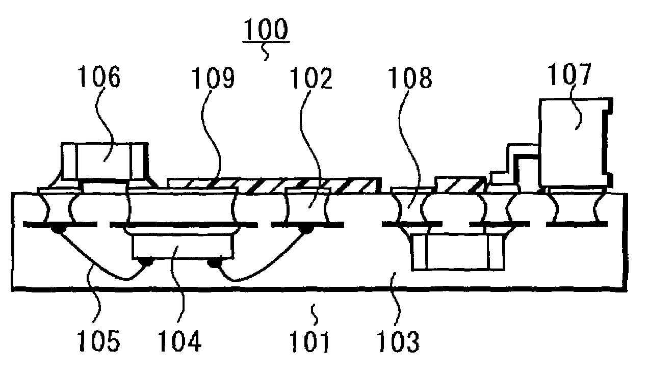
However, this package type semiconductor device 1 had the lead terminal 4 out of the resin layer 3, and was too large in total size to meet smaller, thinner and lighter requirements.
Thereafter, the same manufacturing method of FIG. 26, up to coating the resin layer is followed, but since the ceramic substrate is very fragile, and is likely to break off, unlike a flexible sheet or the glass epoxy substrate, there is a problem with the difficulty of molding using die.
However, only these components were difficult to provide an electrical circuit device reduced in size, thickness and weight.
However, since the manufacturing method involves pasting the electrode on the substrate, the support substrate is required, and this glass epoxy substrate 5 could not be dispensed with.
Further, since the glass epoxy substrate 5 was thick, the circuit device was thick, limiting the possibility to reduce the size, thickness and weight of the device.
Hence, there was a problem with the long manufacturing process.
Accordingly, this slender wire has smaller contact area with the substrate, leading to exfoliation or curvature of the wire.
Particularly, the bonding pad for small signal has a small bonding area, which caused a film exfoliation.
There was a problem that the external lead pad 30 might be exfoliated due to an external force applied to the external lead.
Method used
Image
Click on the blue label to locate the original text in one second.
Reading with bidirectional positioning of images and text.
Examples
first embodiment
for a Manufacturing Method of a Circuit Device
[0138]Referring to FIGS. 3 to 7 and FIG. 1, a manufacturing method of a circuit device 53 will be described below.
[0139]Firstly, a sheet conductive foil 60 is prepared. This conductive foil 60 is composed of a material which is selected in consideration of the adhesive property to the brazing material, bonding property and plating property. Specifically, the material may be Cu or Al as the main constituent, or an alloy of Fe—Ni. Further lamination plate of Cu and Al is applicable.
[0140]The conductive foil is preferably about 10 μm to 300 μm thick in view of the etching that is performed later. Herein, a copper foil having a thickness of 70 μm (2 ounces) is used. However, the thickness may be fundamentally over 300 μm or less than 10 μm. It is sufficient that the trench 61 which has a smaller depth than the thickness of the conductive foil 60 may be formed, as will be described later.
[0141]The sheet laminated conductive foil 60 is rolled ...
second embodiment
for a Manufacturing Method of a Circuit Device
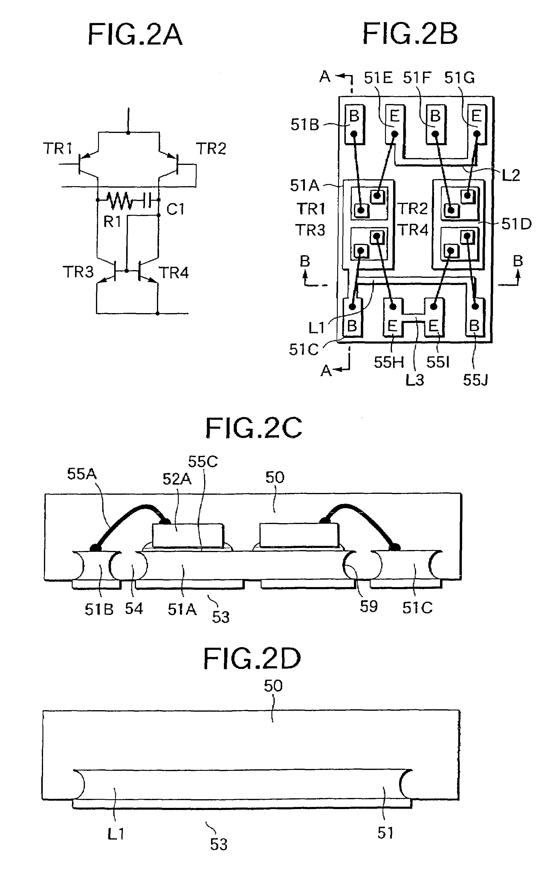
[0170]Referring to FIGS. 9 to 13 and FIG. 8, a manufacturing method of a circuit device 56 having a visor 58 will be described below. The second embodiment is substantially the same as the first embodiment (FIGS. 1 and 2), except that a second material 70 which serves as the visor is applied. The details are not described here.
[0171]Firstly, a laminated conductive foil 60 is prepared in which the second material 70 having a small etching rate is applied on the conductive foil 60 made of the first material, as shown in FIG. 9.
[0172]For example, if Ni is applied on the Cu foil, Cu and Ni can be etched by ferricchloride or cupric chloride at a time, advantageously resulting in the formation of the visor 58 of Ni, due to a difference between etching rates. The bold line indicates the conductive coat 70 made of Ni, its film thickness being preferably about 1 to 10 μm. The larger film thickness of Ni can form the visor 58 more easily.
[0173]Th...
third embodiment
for a Manufacturing Method of a Circuit Device
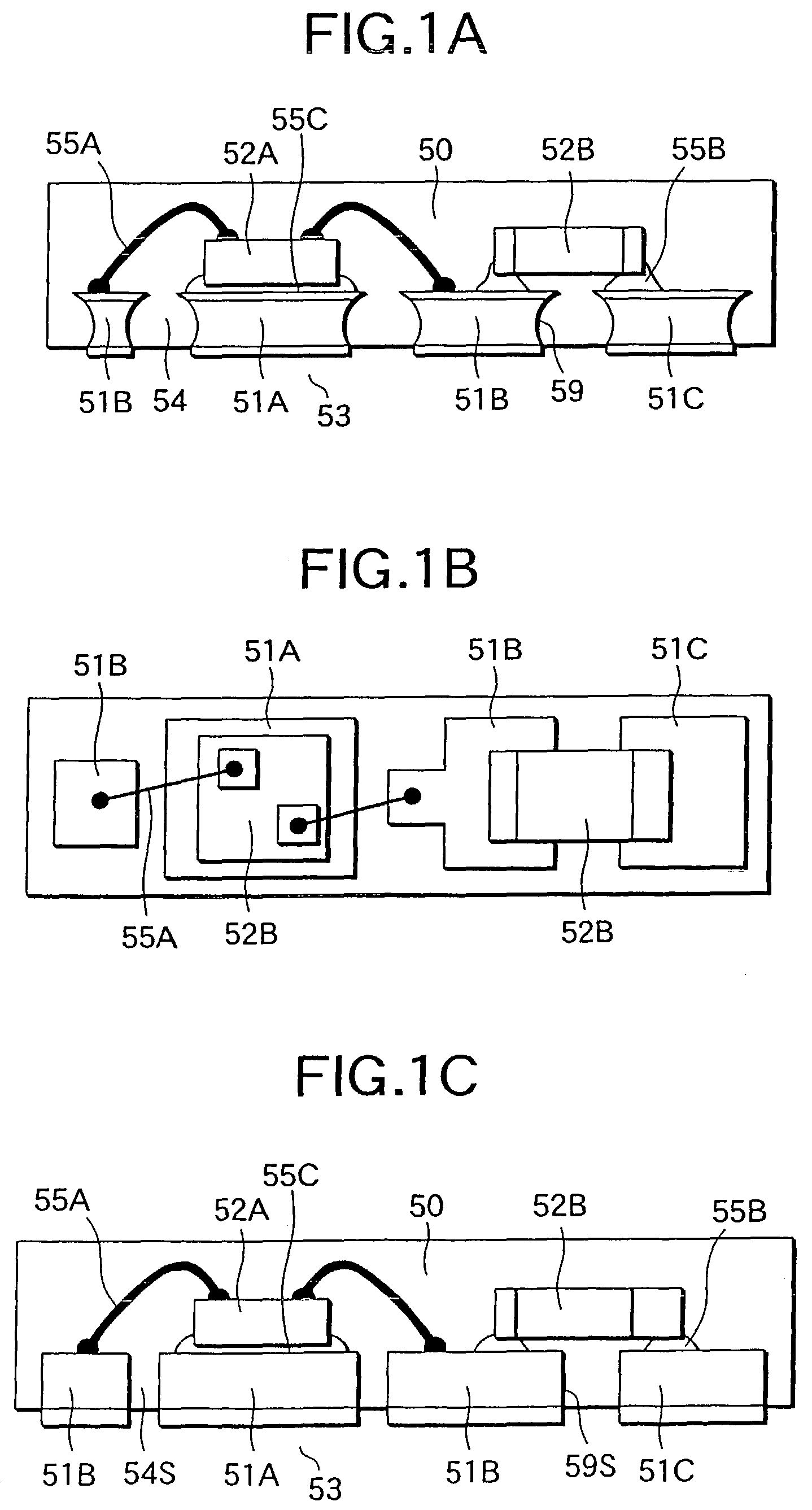
[0178]Referring to FIGS. 14 to 20, a method for manufacturing a circuit device will be described below, in which the IC circuits having the conductive paths composed of a plurality of kinds of circuit elements, wires, die pads and bonding pads are arranged like a matrix and divided into individual IC circuits after sealing. Referring to FIG. 2 and particularly a cross-sectional view of FIG. 2C, the structure will be described below. This manufacturing method is substantially the same as in the first embodiment and the second embodiment, and is simply described.
[0179]Firstly, a sheet conductive foil 60 is prepared, as shown in FIG. 14.
[0180]The sheet conductive foil 60 is rolled in a predetermined width, and maybe carried to the later process. Or the conductive foils cut in a predetermined size may be prepared and carried to the later process.
[0181]Subsequently, there is a step of removing the conductive foil 60 except for at least the re...
PUM
Abstract
After a trench 54 is formed in a conductive foil 60, the circuit elements are mounted, and the insulating resin is applied on the conductive foil 60 as the support substrate. After being inverted, the conductive foil 60 is polished on the insulating resin 50 as the support substrate for separation into the conductive paths. Accordingly, it is possible to fabricate the circuit device in which the conductive paths 51 and the circuit elements 52 are supported by the insulating resin 50, without the use of the support substrate. And the interconnects L1 to L3 requisite for the circuit are formed, and can be prevented from slipping because of the curved structure 59 and a visor 58.
Description
[0001]This application is a continuation-in-part of U.S. application Ser. No. 09 / 671,135, filed Sep. 27, 2000 now U.S. Pat. No. 6,548,328, which in turn claims the benefit of Japanese priority applications, serial no. 2000-022646, filed Jan. 31, 2000, serial no. 2000-24047, filed Feb. 1, 2000, serial no. 2000-32417, filed Feb. 9, 2000, and serial no. 2000-32454, filed Feb. 9, 2000. The disclosures of the prior applications are considered part of and are incorporated by reference in the disclosure of this application.BACKGROUND OF THE INVENTION[0002]1. Field of the Invention[0003]The present invention relates to a circuit device and a method for manufacturing the circuit device and a semiconductor module, and more particularly to a thin-type circuit device and a method of manufacturing the thin-type circuit device without the need of providing a support substrate, and a semiconductor module with the circuit device.[0004]2. Description of the Related Art[0005]Conventionally, it has be...
Claims
Application Information
Patent Timeline
Application Date:The date an application was filed.
Publication Date:The date a patent or application was officially published.
First Publication Date:The earliest publication date of a patent with the same application number.
Issue Date:Publication date of the patent grant document.
PCT Entry Date:The Entry date of PCT National Phase.
Estimated Expiry Date:The statutory expiry date of a patent right according to the Patent Law, and it is the longest term of protection that the patent right can achieve without the termination of the patent right due to other reasons(Term extension factor has been taken into account ).
Invalid Date:Actual expiry date is based on effective date or publication date of legal transaction data of invalid patent.

