Resonator device, filter, duplexer and communication device

a communication device and filter technology, applied in the direction of resonators, electrical equipment, waveguides, etc., can solve the problems of reducing the insertion loss of an rf transmission-reception portion, the inability of resonators with high no-load q (q0) to form, and the inability to form a resonator with high no-load q (q0). , to achieve the effect of reducing the loss of an rf transmission-

Active Publication Date: 2006-08-22
MURATA MFG CO LTD
View PDF4 Cites 15 Cited by
  • Summary
  • Abstract
  • Description
  • Claims
  • Application Information

AI Technical Summary

Benefits of technology

[0008]It is an object of the present invention to provide a resonator device, filter, duplexer, and communication device having a high Q0 resonator to be obtained by reducing the conductor loss in the above capacitor (capacitive area).

Problems solved by technology

When such a magnetic-field vector has a locally sharp curvature, the conductor loss of a real current flowing in conductor lines is produced to cause the deterioration of electrical characteristics.
Then, when a resonator is constituted by combining such an interdigital capacitor to an inductor, there is a problem in that a resonator having high no-load Q (Q0) cannot be formed.
Furthermore, when capacitors are constructed by forming fine thin-film conductor lines on a dielectric substrate, although the density can be increased, a practical construction has not been disclosed to form inductors for comprising a resonator and to perform input and output to the outside.

Method used


Image

  • Resonator device, filter, duplexer and communication device
  • Resonator device, filter, duplexer and communication device
  • Resonator device, filter, duplexer and communication device

Examples


first embodiment

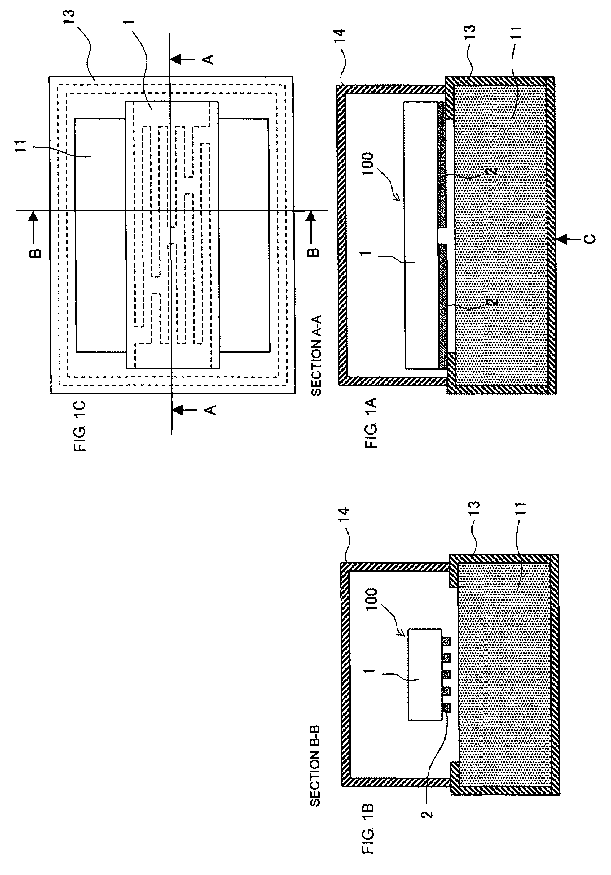
[0059]FIGS. 1A to 1C show a resonator device according to the present invention. FIG. 1C is a top view of the resonator device with an upper shielding cap 14 removed, FIG. 1A is a sectional view taken on line A—A of FIG. 1C, and FIG. 1B is a sectional view taken on line B—B of FIG. 1C. This resonator device contains a dielectric substrate 1 having conductor lines 2 formed thereon, a mounting substrate 11 having a shielding electrode 13 formed thereon, and a shielding cap 14.

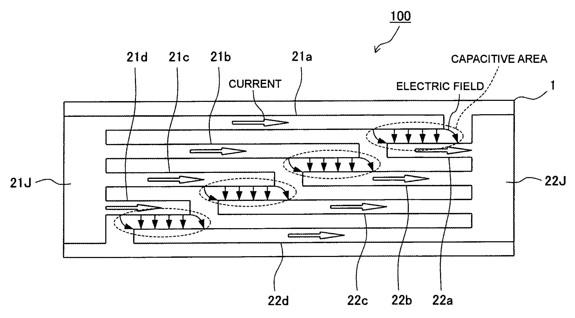
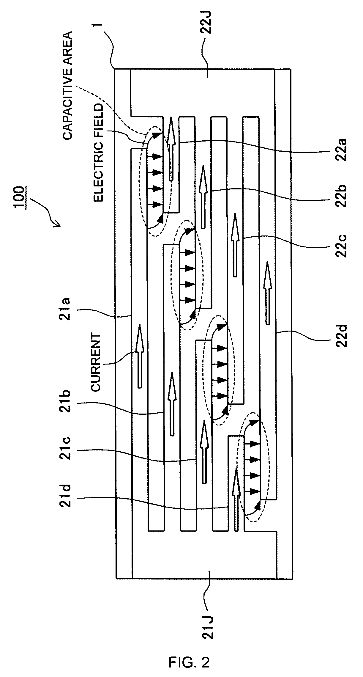
[0060]A high-frequency circuit element 100 is constructed by forming the conductor lines 2 on the dielectric substrate 1. No grounding electrode is formed on the surface of the dielectric substrate 1 opposite to the surface where the conductor lines 2 are formed. The high-frequency circuit element 100 functions as capacitive areas and a part of inductive areas. Furthermore, the shielding electrode 13 formed on the mounting substrate 11 and the shielding cap 14 function as a part of the inductive areas. The shield...

third embodiment

[0086]FIGS. 5A and 5B show a dielectric substrate used in a resonator device according to the present invention. In the examples shown in FIGS. 2 and 4, four capacitive areas are contained, but, in examples shown in FIGS. 5A and 5B, the number of capacitive areas is increased and the line width of each conductor line is made different. In the example shown in FIG. 5A, eight sets of conductor lines 21a to 21h and 22a to 22h and eight captive areas enclosed by broken lines in the drawing are formed. One end of these conductor lines 21a to 21h is commonly connected to the connection portion 21J and one end of these conductor lines 22a to 22h is commonly connected to the connection portion 22J.

[0087]FIG. 5B shows an example in which the number of neighboring end portions in the width direction of conductor lines, that is, the number of capacitive areas, are increased.

[0088]Furthermore, in the examples shown in FIGS. 5A and 5B, the width of the conductor lines are gradually reduced from ...

sixth embodiment

[0099]FIGS. 9A and 9B are a top view and a sectional view of a high-frequency circuit element 100 according to the present invention. In the example shown in FIG. 7C, the capacitive areas 30a to 30e are disposed substantially in the middle of the dielectric substrate 1, but, in the example in FIG. 9, the end portions of the conductor lines 22a to 22e are made close in the thickness direction to the connection portion 21J through a dielectric layer.


PUM


Abstract

A resonator device including a plurality of resonance units formed on a dielectric substrate, each resonance unit having a plurality of conductor lines forming a capacitive area and an inductive area in a ring shape.

Description

BACKGROUND OF THE INVENTION[0001]1. Field of the Invention[0002]The present invention relates to a resonator device, filter, duplexer, and communication device which are used in radio communication in microwave band and millimeter wave band and in transmission and reception of electromagnetic waves, for example.[0003]2. Description of the Related Art[0004]Up to now, as a capacitor used in an integrated high-frequency circuit, an interdigital capacitor, in which two strip conductors having a plurality of fingers are disposed so as to face each other on a dielectric substrate, is disclosed in Japanese Unexamined Patent Application Publication No. 60-1825.[0005]In the interdigital capacitor disclosed in Japanese Unexamined Patent Application Publication No. 60-1825, the fingers (comb-shaped electrodes) are alternately arranged to have a interdigital-type structure and the electric-field vectors generated in the space between neighboring two electrodes are alternately reversed. The stat...

Claims


Application Information

Patent Timeline
Patent Type & Authority Patents(United States)
IPC IPC(8): H01P7/00H03H5/02H01P1/201H01P7/08H03H7/01H03H7/46H04B1/50
CPCH01P7/082H01P1/201
Inventor HIDAKA, SEIJIABE, SHIN
Owner MURATA MFG CO LTD
Why Eureka
Try Eureka