Embedded duo-planar printed inductor

a duo-planar printed and inductor technology, applied in the field of inductor, can solve the problems of reducing reducing the effective inductance, and typically unsatisfactory effects, so as to reduce the q value of components and reduce the effective inductance

Active Publication Date: 2006-08-10
NORTHROP GRUMMAN SYST CORP
View PDF6 Cites 13 Cited by
  • Summary
  • Abstract
  • Description
  • Claims
  • Application Information

AI Technical Summary

Benefits of technology

[0007] The present invention resides in a printed inductor structure formed in two planar layers of a printed circuit board. Briefly, and in general terms, the inductor structure of the invention comprises a dielectric substrate having upper and lower faces; a first set of parallel conductive traces formed on the upper face of the substrate; a second set of parallel conductive traces formed on the lower face of the substrate; and a plurality of metallized vias extending through the substrate and interconnecting the first and second sets of conductive traces to form a horizontal continuous spiral path with desirable (low loss, high Q) inductive properties.
[0012] Due to the highly contained magnetic fields, similar to a toroid, the presence of nearby metallic, or otherwise conducting structures forming a return AC or RF path, is less pronounced. The reduced “lid effect” thus is presented and increases realized Q and increases the structures self-resonant operating frequency: both very desirable from a circuit standpoint (better LC filter: lower loss, better selectivity, as an example). Further the physical implementation thus allows tighter, more volume efficient construction techniques, otherwise unobtainable from conventional solenoidal implementations.

Problems solved by technology

Although some of these structures may be designed to have a relatively high Q value, a common drawback to the latter structures is that surrounding metal structures acting as RF or AC return paths effectively lower the Q value, referred to as “de-Qing.” This phenomenon is also referred to as the “lid effect” when filters are placed in metal cavities.
This undesirable effect typically arises because of parasitic capacitances to ground.
Currents are induced in these structures, reducing the effective inductance, and also reducing the components' Q value.
Unfortunately, increasing the cross-sectional area or the number of turns is not consistent with the goal of compactness, and one drawback of adding high permittivity material is that the increase in inductance value is obtained at a cost of a lower effective Q factor.

Method used


Image

  • Embedded duo-planar printed inductor
  • Embedded duo-planar printed inductor
  • Embedded duo-planar printed inductor

Examples


Embodiment Construction

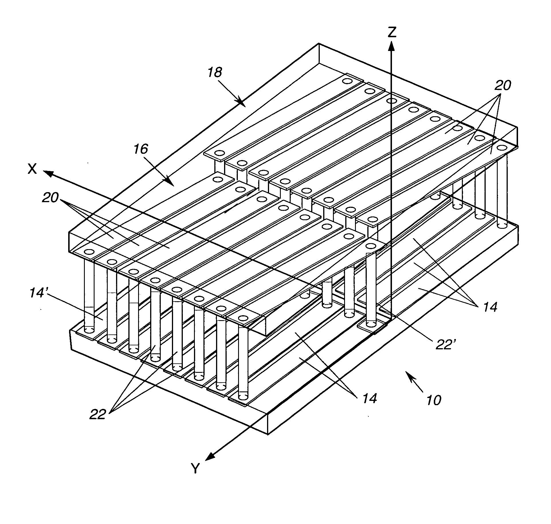
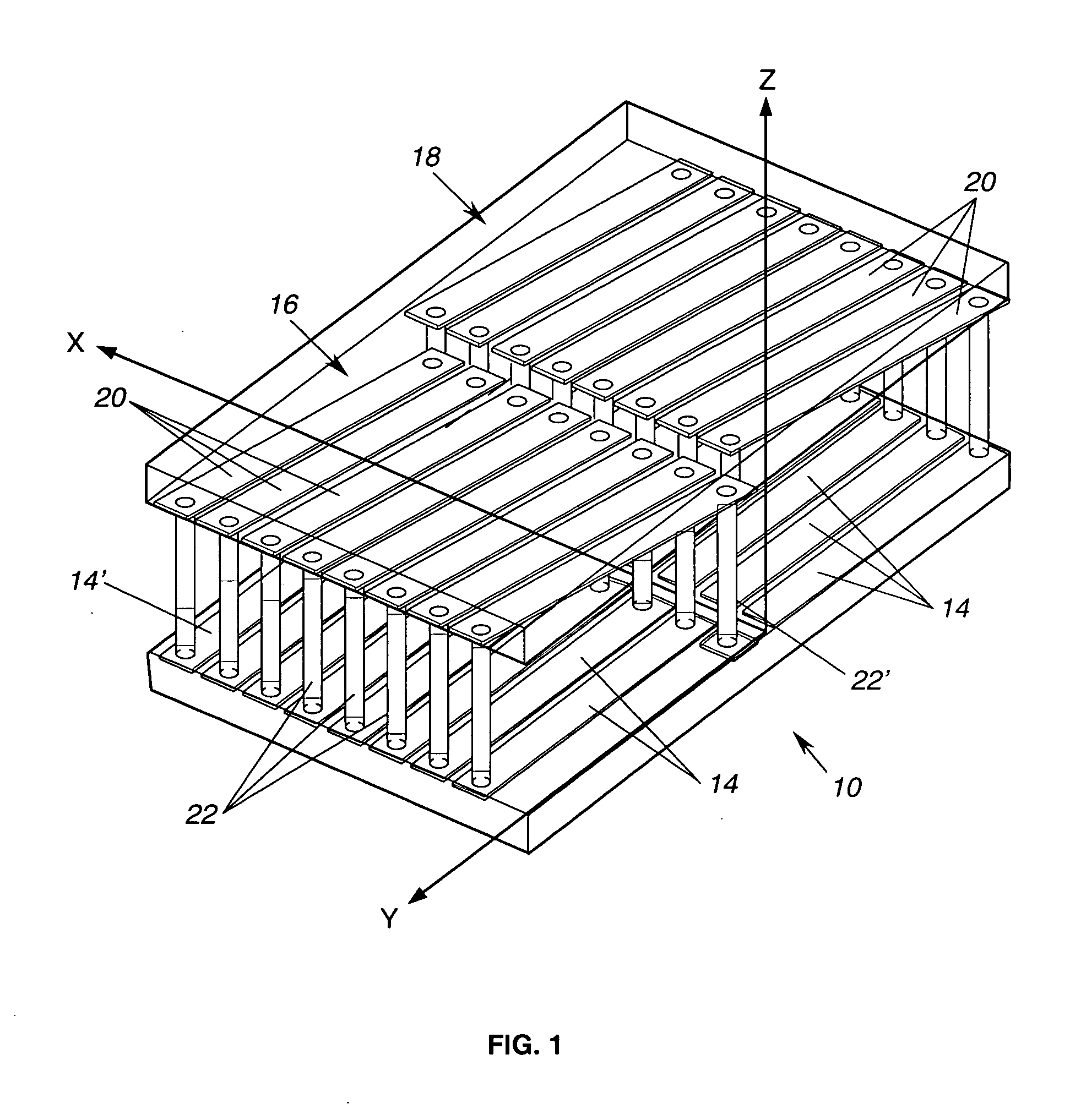
[0022] As shown in the drawings for purposes of illustration, the present invention is concerned with printed inductors formed on a printed circuit board structure. Prior to this invention, printed inductors used spiral traces or traces of other shapes on a single metallized layer of a printed circuit board. Alternatively, wire-coiled inductors may be surface mounted on a printed circuit board. Neither of these solutions has been able to achieve desirably high values of inductance and a lower frequency contourable Q in a compact structure.

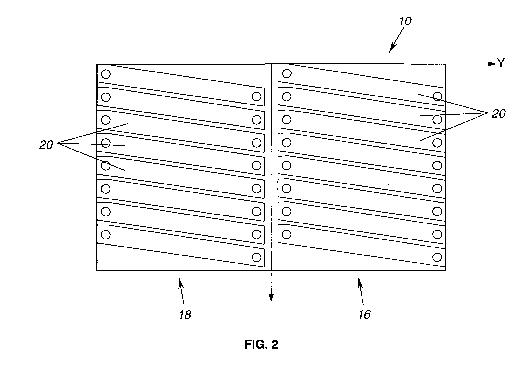
[0023] In accordance with the present invention, a printed inductor takes the form of conductive traces in two parallel planar layers of a printed circuit board structure, the conductive traces being electrically connected by metal vias extending between the two planar layers. The details of this construction are best shown in the perspective view of FIG. 1, considered in conjunction with the top view, lateral view and front view of FIGS. 2-4, res...


PUM

PropertyMeasurementUnit
capacitanceaaaaaaaaaa
frequencyaaaaaaaaaa
frequencyaaaaaaaaaa

Abstract

A highly compact inductor formed on opposite faces of a dielectric substrate. Sets of parallel spaced conductive traces formed on the opposite faces of the substrate are interconnected by metallized vias through the substrate, in such a way as to form a continuous spiral conductive path. The inductor is preferably formed as two closely adjacent segments, each with conductive traces on each face of the substrate and each having metallized vias interconnecting the conductive traces. The segments are electrically connected in series and produce a magnetic field that extends through each segment in opposite directions and is closely coupled from one segment to the other. The inductor is, therefore, electromagnetically similar to a wire-wound toroidal inductor, providing high inductance and contourable Q values, but is highly compact, especially in the z-axis direction normal to the substrate.

Description

BACKGROUND OF THE INVENTION [0001] This invention relates generally to inductors of compact design and, more particularly, to inductors that can be fabricated in printed circuit form. Conventional inductor technology for high-frequency (HF) filters, typically in the 10s of Megahertz (MHz), require filter inductor values as high as one or two microhenries (uH). Physical realization of inductance can be achieved in a number of ways, but is largely dependent upon the inductor application; the frequency of operation and available physical space. In general, achieving a larger value of inductance requires a physical inductor with a larger volume. A larger volume also results in an inductor with a higher quality factor (Q). The Q of an inductor may be thought of as the ratio of the reactance of the inductor (measured by the product ωL, where ω is angular frequency and L is the inductance) to the resistance of the inductor. Q is also defined, in the context of a tuned circuit or a filter, ...

Claims


Application Information

Patent Timeline
Patent Type & Authority Applications(United States)
IPC IPC(8): H01F5/00
CPCH01F17/0033H01F41/041Y10T29/4902H05K1/165H05K2201/097H01F2017/002
Inventor WINTER, FRANK B.HARBERTS, HARRY S.TOLAN, JULIUS G.
Owner NORTHROP GRUMMAN SYST CORP
Why Eureka
Try Eureka