Fully differential, high Q, on-chip, impedance matching section

a technology of impedance matching and fully differential, applied in the field of impedance matching and impedance transformation, can solve the problems of reducing affecting the performance of the lna, and affecting the efficiency of the lna, so as to reduce the size of the match circuit footprint, reduce the loss of signal, and high q

Inactive Publication Date: 2006-08-22
AVAGO TECH WIRELESS IP SINGAPORE PTE
View PDF5 Cites 20 Cited by
  • Summary
  • Abstract
  • Description
  • Claims
  • Application Information

AI Technical Summary

Benefits of technology

[0018]Embodiments of the present invention take advantage of the electromagnetic properties of differential inductors to reduce the size of the match circuit footprint. That is, because the inductance is higher in the interleaved differential inductor of the embodiments of the present invention, the interleaved differential inductor can have a high Q while being made smaller than conventional impedance matching inductor pairs. Thus, less metal is needed in each differential path through the interleaved differential inductor. Since loss is increased by the amount of metal traversed in a signal path, the interleaved differential inductor reduces signal loss. Other aspects and advantages of the invention will become apparent from the following detailed description, taken in conjunction with the accompanying drawings, illustrating by way of example the principles of the invention.

Problems solved by technology

However, when the impedance is not matched, the performance, such as output power, efficiency, linearity, etc., of the LNA is degraded, as illustrated in FIG. 1.
As a result, the signal transfer 108 will be reduced and emissions problems may occur if the reflection is too large.
Unfortunately, discreet match components add extra cost and occupy valuable board space.
For a differential LNA as illustrated in FIG. 2, two inductors are needed, which further increases the costs and the space required for the inductors.

Method used


Image

  • Fully differential, high Q, on-chip, impedance matching section
  • Fully differential, high Q, on-chip, impedance matching section
  • Fully differential, high Q, on-chip, impedance matching section

Examples


Embodiment Construction

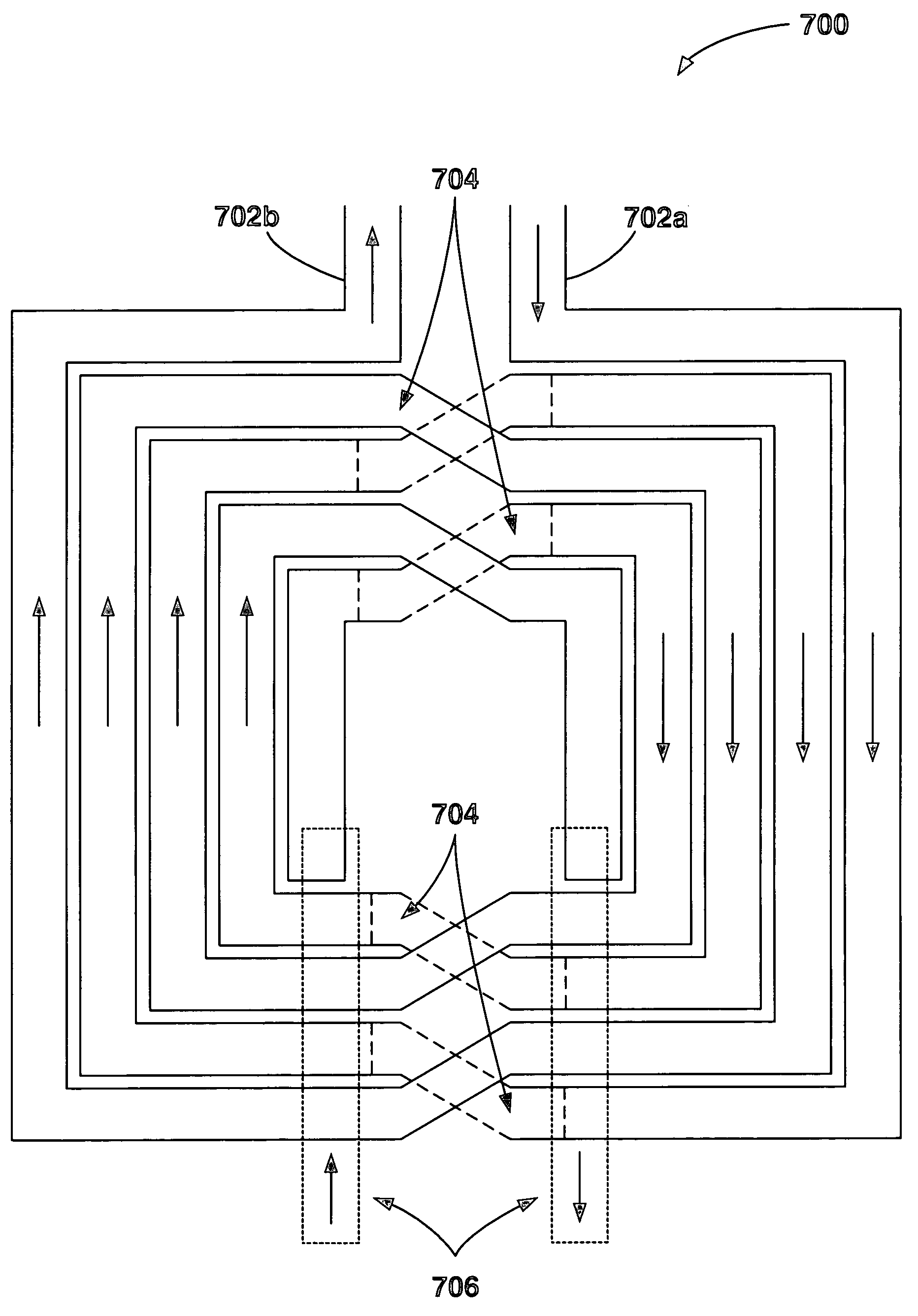
[0029]An invention is disclosed for a fully differential, high-Q, on-chip impedance matching section. Generally speaking, embodiments of the present invention provide impedance matching using an interleaved differential inductor. The interleaved differential inductor is comprised of two inductors, wherein one of the inductors is flipped about the center axis and interleaved with the other inductor. In the following description, numerous specific details are set forth in order to provide a thorough understanding of the present invention. It will be apparent, however, to one skilled in the art that the present invention may be practiced without some or all of these specific details. In other instances, well known process steps have not been described in detail in order not to unnecessarily obscure the present invention.

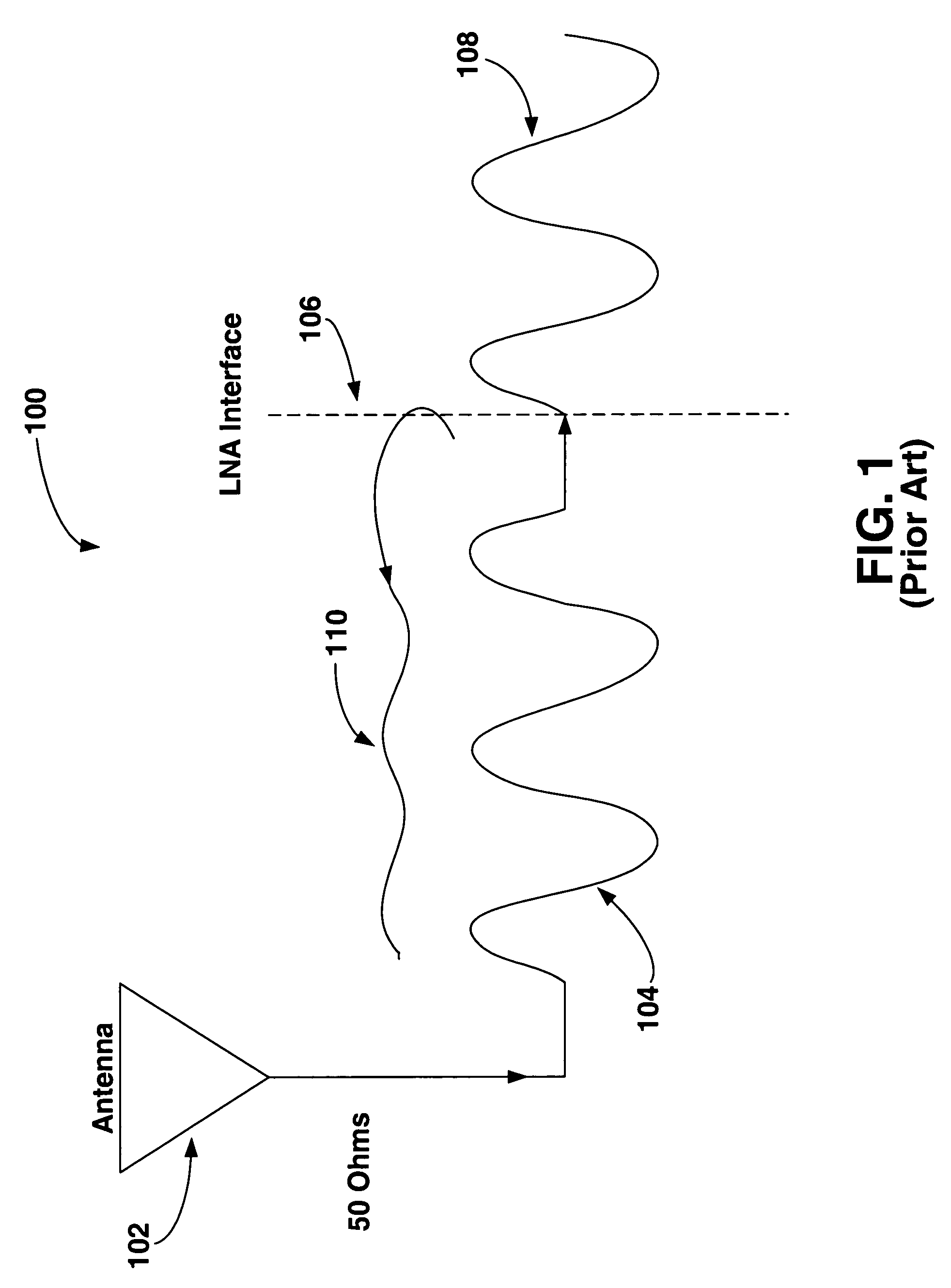
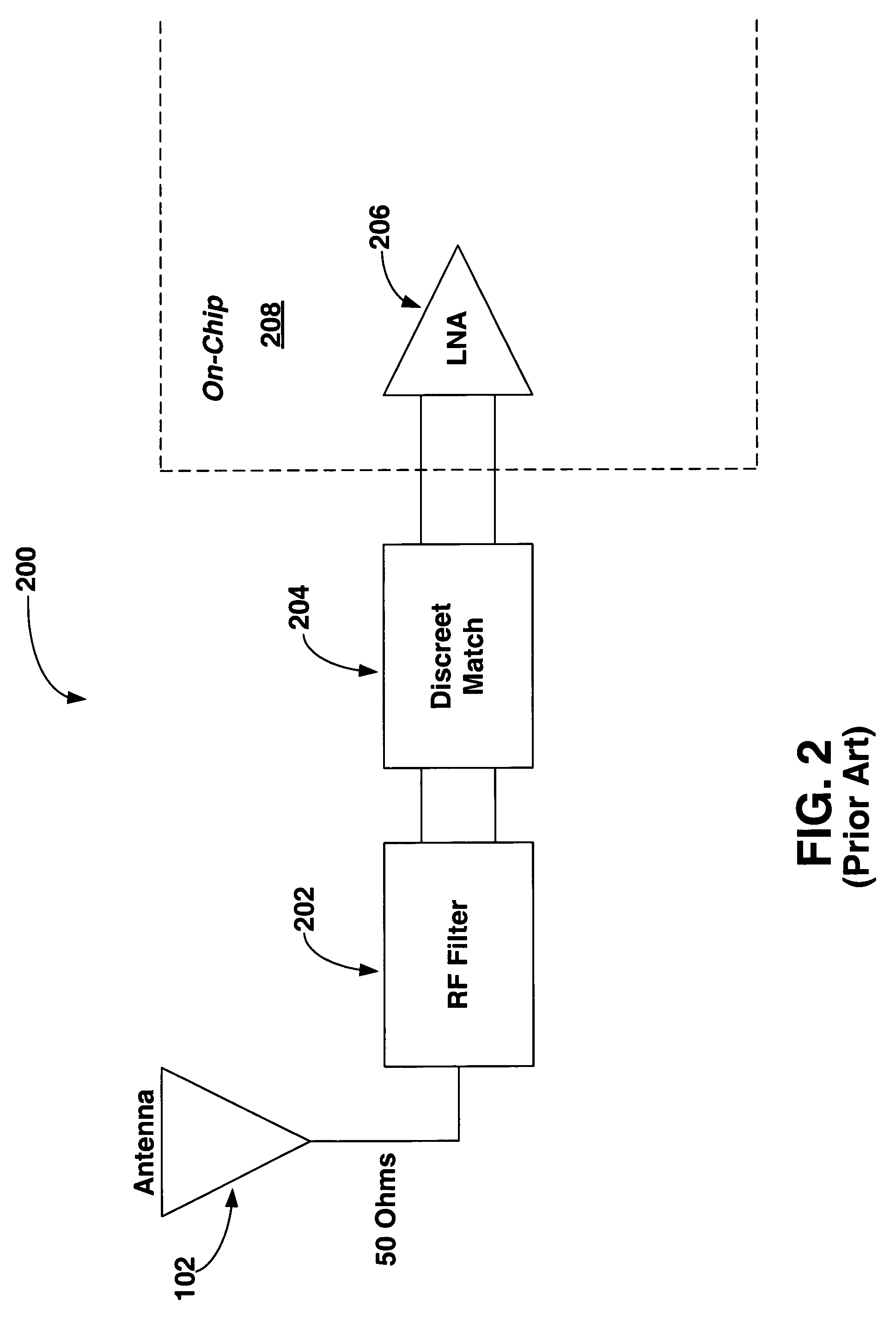
[0030]As discussed above, radio frequency integrated circuits (RF ICs) generally are designed to include inductors for impedance matching. The inductance and quality fa...


PUM

PropertyMeasurementUnit
impedancesaaaaaaaaaa

Abstract

An inductor circuit is disclosed. The inductor circuit includes a first in-silicon inductor and a second in-silicon inductor each having multiple turns. A portion of the multiple turns of the second in-silicon inductor is formed between turns of the first in-silicon inductor. The first and second in-silicon inductors are configured such that a differential current flowing through the first in-silicon inductor and the second in-silicon inductor flows in a same direction in corresponding turns of inductors.

Description

BACKGROUND OF THE INVENTION[0001]1. Field of the Invention[0002]This invention relates generally to impedance matching and impedance transformation, and more particularly to differential impedance matching and transformation.[0003]2. Description of the Related Art[0004]Impedance matching circuits generally are utilized to efficiently transfer energy at a junction point where electronic circuits having different characteristic impedances are connected to each other. This is accomplished by rendering the impedances seen on either side of the junction point identical, that is, to match line impedances and load impedances of the circuits.[0005]Such line impedance matching is necessary not only for a wire terminal but also for a wireless terminal, wherein the impedances are matched at 50, 75 and 100 Ohms according to convention and the characteristics of the antenna and transmission lines. For example, radio frequency (RF) circuits often utilize a low noise amplifier (LNA) to amplify a r...

Claims


Application Information

Patent Timeline
Patent Type & Authority Patents(United States)
IPC IPC(8): H01F5/00
CPCH01L23/5227H01F2017/0046H01L2924/3011H01L2924/0002H01L2924/00
Inventor BARRETT, CAROLMCKAY, TOMBOTHRA, SUBHAS
Owner AVAGO TECH WIRELESS IP SINGAPORE PTE
Why Eureka
Try Eureka