Apparatus for manufacturing bonded substrate

a technology of bonded substrates and apparatuses, which is applied in the direction of mechanical control devices, process and machine control, instruments, etc., can solve the problems of shortening the time consumed for operation, the vacuum chuck cannot hold, and the treatment chamber cannot be depressurized optimally, etc., and achieves the effect of suppressing defects

Inactive Publication Date: 2006-08-29
FUJITSU LTD
View PDF50 Cites 20 Cited by
  • Summary
  • Abstract
  • Description
  • Claims
  • Application Information

AI Technical Summary

Benefits of technology

[0029]Accordingly, it is an objective of the present invention to provide an apparatus for manufacturing a bonded substrate that suppresses a defect in a resulting product.

Problems solved by technology

As compared to the vacuum method, the drip method requires less liquid crystal and shortens the time consumed for the operation.
However, an apparatus for manufacturing a panel display in accordance with the drip method has the following problems.
However, if the treatment chamber is depressurized sufficiently, the holding performance of the vacuum chuck is lowered and the vacuum chuck cannot hold each substrate 11, 16 in a stable manner.
To avoid this, the treatment chamber cannot be depressurized optimally.
As a result, the substrates 11, 16 are bonded together non-uniformly, thus causing a display defect in a resulting product.
This reduces the aperture ratio of each pixel (TFT) 13 or causes a problem such as a light leakage from a shielded portion.
This damages a circuit or TFTs formed on each substrate 11, 16, thus causing a defective product.
The liquid crystal thus cannot meet a requirement that an LCD with TFTs should have a relatively high voltage maintaining rate.
This causes display non-uniformness, particularly in half tone.
In these cases, the opposed substrates 11, 16 are bonded together as misaligned, thus leading to a defect in the cell gap.
Accordingly, it is complicated to manufacture the panel display 10 in a stable manner.
These factors vary the drip amount for each drip position, and the resulting cell thickness becomes non-uniform.
This causes display non-uniformness near the periphery of the panel display.
In this state, display non-uniformness is caused in the entire panel display.
However, this lens has a complicated structure and is sometimes unavailable.
This makes the bonding procedure difficult, and a defect may be caused in the bonded substrates 11, 16.
However, a pressing device, such as a hydraulic cylinder, is located outside the treatment chamber and is exposed to the atmospheric air.
However, for example, aging of the pressing device may alter the pressure applied to the substrates 11, 16.
This hampers reproducibility of the bonding.

Method used


Image

  • Apparatus for manufacturing bonded substrate
  • Apparatus for manufacturing bonded substrate
  • Apparatus for manufacturing bonded substrate

Examples


Embodiment Construction

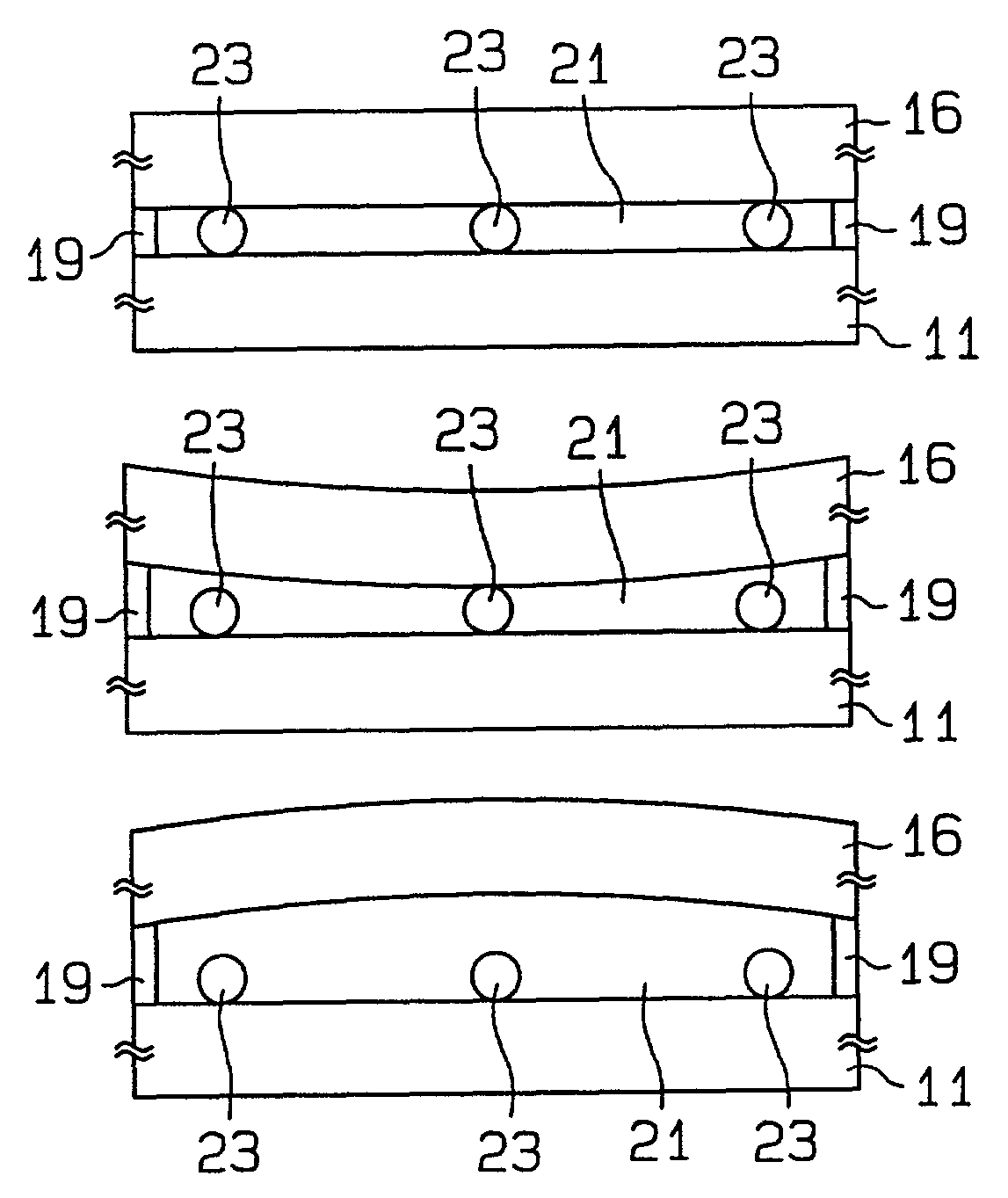
[0072]A bonded substrate manufacturing apparatus 30 of an embodiment according to the present invention will now be described with reference to FIGS. 5 to 22.

[0073]FIG. 5 is a view schematically showing the apparatus 30 that is used in a cell step of a process for fabricating a liquid crystal panel display. In the cell step, liquid crystal is dripped on a substrate, and the substrate is bonded with an opposed substrate.

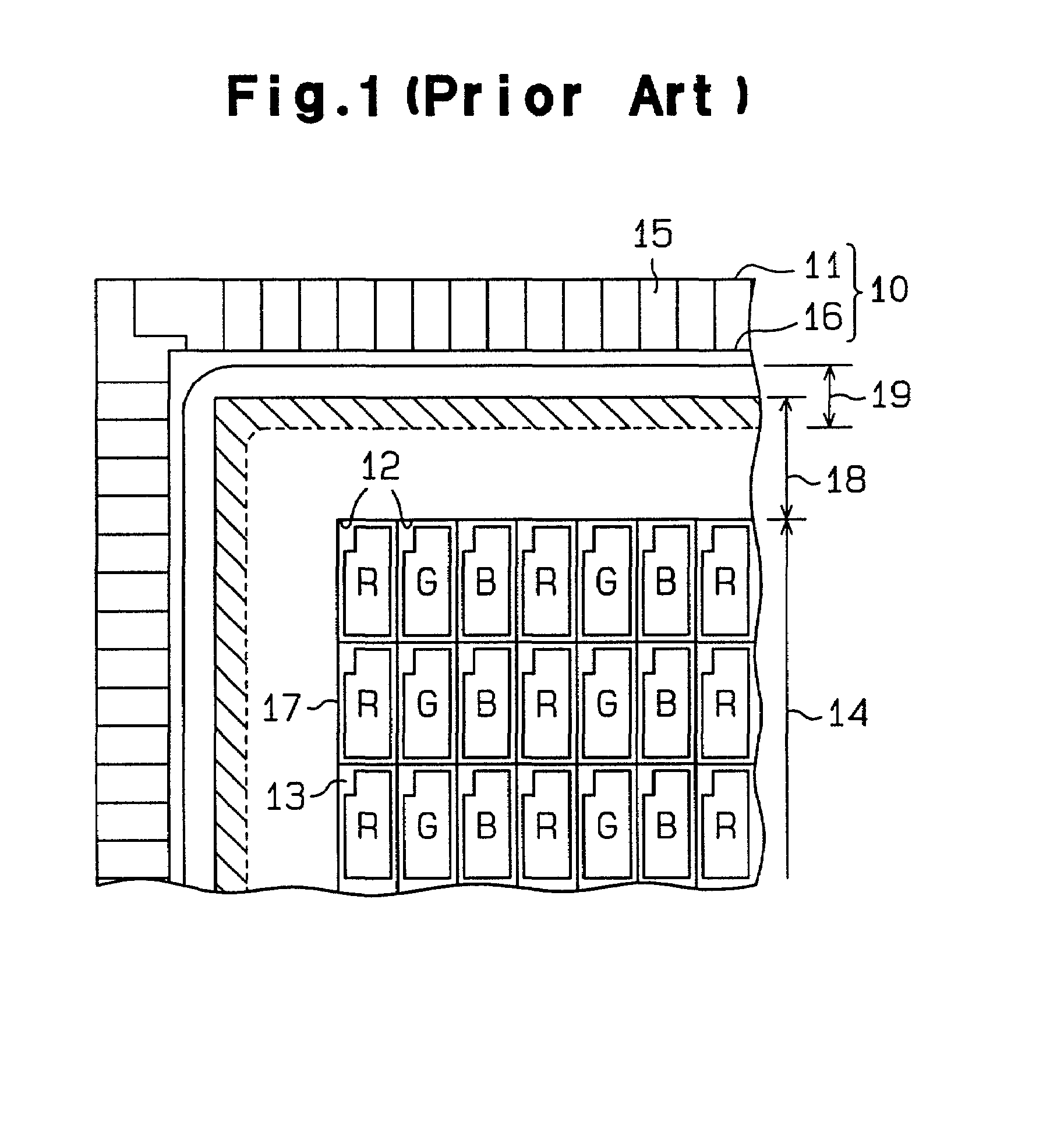
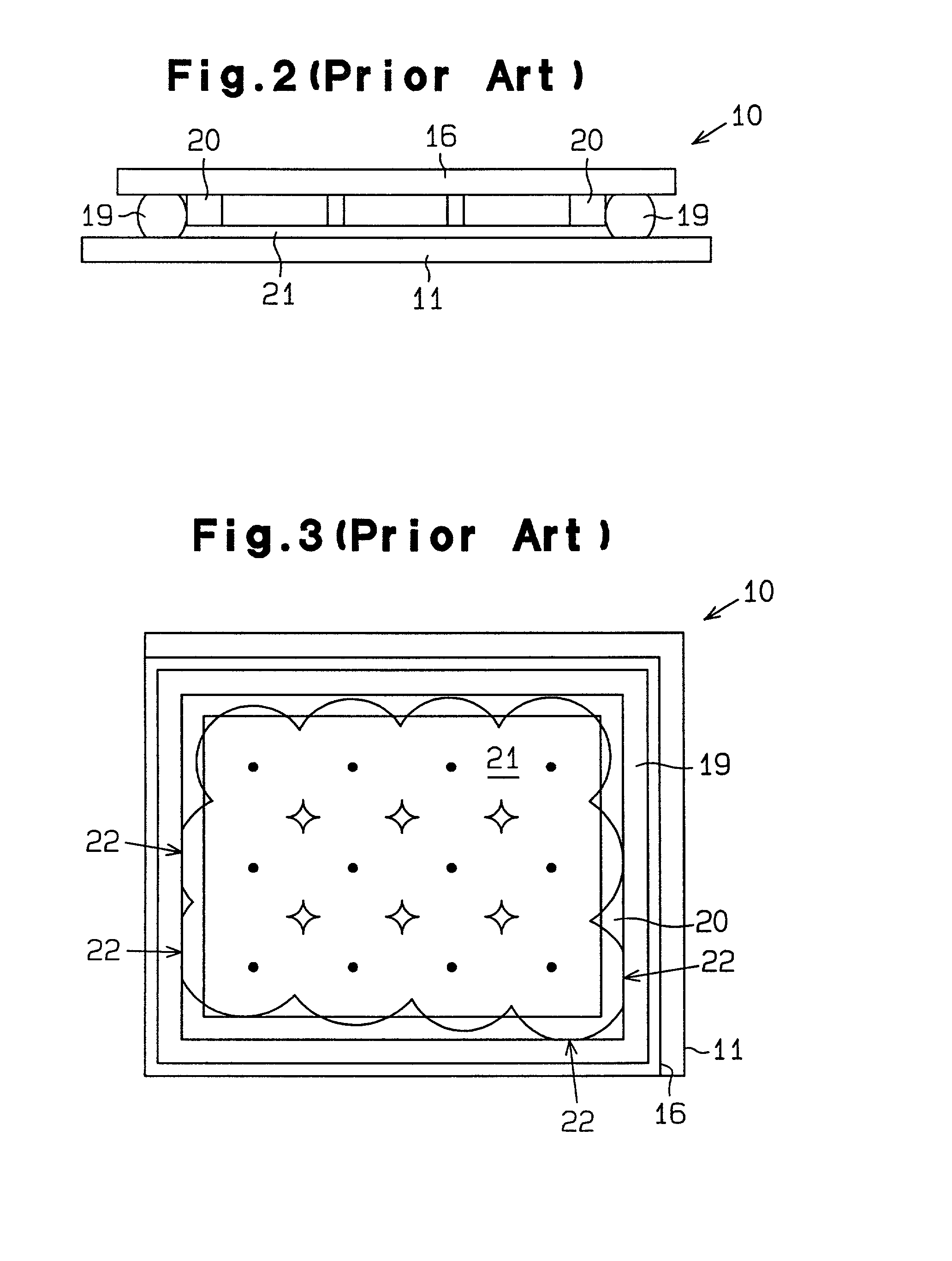
[0074]In the liquid crystal panel display fabricated with the bonded substrate manufacturing apparatus 30, liquid crystal is filled in the gap between a first substrate W1 and a second substrate W2. If the panel display is an active matrix type, the first substrate W1 is a glass array substrate that includes switch elements such as TFTs, and the second substrate W2 is a color filter (CF) substrate that includes a color filter or a shielding film. The first substrate W1 and the second substrate W2 are fabricated in separate steps and are supplied to the apparatus 30. A...


PUM

PropertyMeasurementUnit
flatnessaaaaaaaaaa
depthaaaaaaaaaa
diameteraaaaaaaaaa

Abstract

The present invention provide an apparatus for manufacturing a bonded substrate that suppresses a defect in the bonded substrate. When the pressure in a vacuum chamber is at the atmospheric level, upper and lower chuck units respectively attract substrates through vacuum. When the vacuum chamber is depressurized, each chuck unit electrostatically attracts the associated substrate. During the depressurization of the vacuum chamber, the pressure for attracting each substrate to the associated chuck unit is controlled to be equal to the pressure in the vacuum chamber. This prevents each substrate from falling from or moving relative to the associated chuck unit. The first and second substrates are thus bonded together as accurately aligned.

Description

BACKGROUND OF THE INVENTION[0001]The present invention relates to apparatuses for manufacturing bonded substrates, and, more particularly, to apparatuses for manufacturing panel displays that have a predetermined gap between a pair of substrates, for example, liquid crystal displays (LCDs).[0002]Panel displays such as LCDs with larger display areas are now being developed. Further, to improve the resolution, an increased pixel count per unit area is demanded in the panel displays. Accordingly, an apparatus for manufacturing panel displays with bonded substrates must be capable of accurately aligning the substrates even if each substrate is relatively large.[0003]FIG. 1 is a plan view showing a portion of a prior art, active-matrix type liquid crystal panel display 10, as viewed from a color filter substrate.[0004]The liquid crystal panel display 10 includes an array substrate 11 and a color filter (CF) substrate 16. The array substrate 11 has a plurality of pixel areas 12 that are f...

Claims


Application Information

Patent Timeline
Patent Type & Authority Patents(United States)
IPC IPC(8): B32B37/00G02F1/1339G02F1/13G02F1/1341
CPCB32B38/1841G02F1/1339G02F1/1341B32B37/12Y10T156/1089B32B2037/1253B32B2038/1891B32B2310/0806B32B2457/20B32B2457/202G02F2001/133354G02F2001/13415Y10T156/1092Y10T29/49776Y10T156/17Y10T156/1798B32B37/18G02F1/133354G02F1/13415G02F1/13
Inventor HASHIZUME, KOJIMIYAJIMA, YOSHIMASAHATANO, NORIHIKOKADOWAKI, TETSUJI
Owner FUJITSU LTD
Why Eureka
Try Eureka