Supercharge Your Innovation With Domain-Expert AI Agents!

Gate triggered ESD clamp

a technology of esd power clamp and gate, which is applied in the direction of pulse manipulation, emergency protective arrangements for limiting excess voltage/current, pulse technique, etc., can solve the problems of fast ramp rate of the voltage between vcc and vss during an esd event, and difficulty in ensuring that the esd power clamp will turn on before other devices connected between vcc and vss are damaged

Inactive Publication Date: 2006-08-29
ALTERA CORP
View PDF9 Cites 18 Cited by
  • Summary
  • Abstract
  • Description
  • Claims
  • Application Information

AI Technical Summary

Benefits of technology

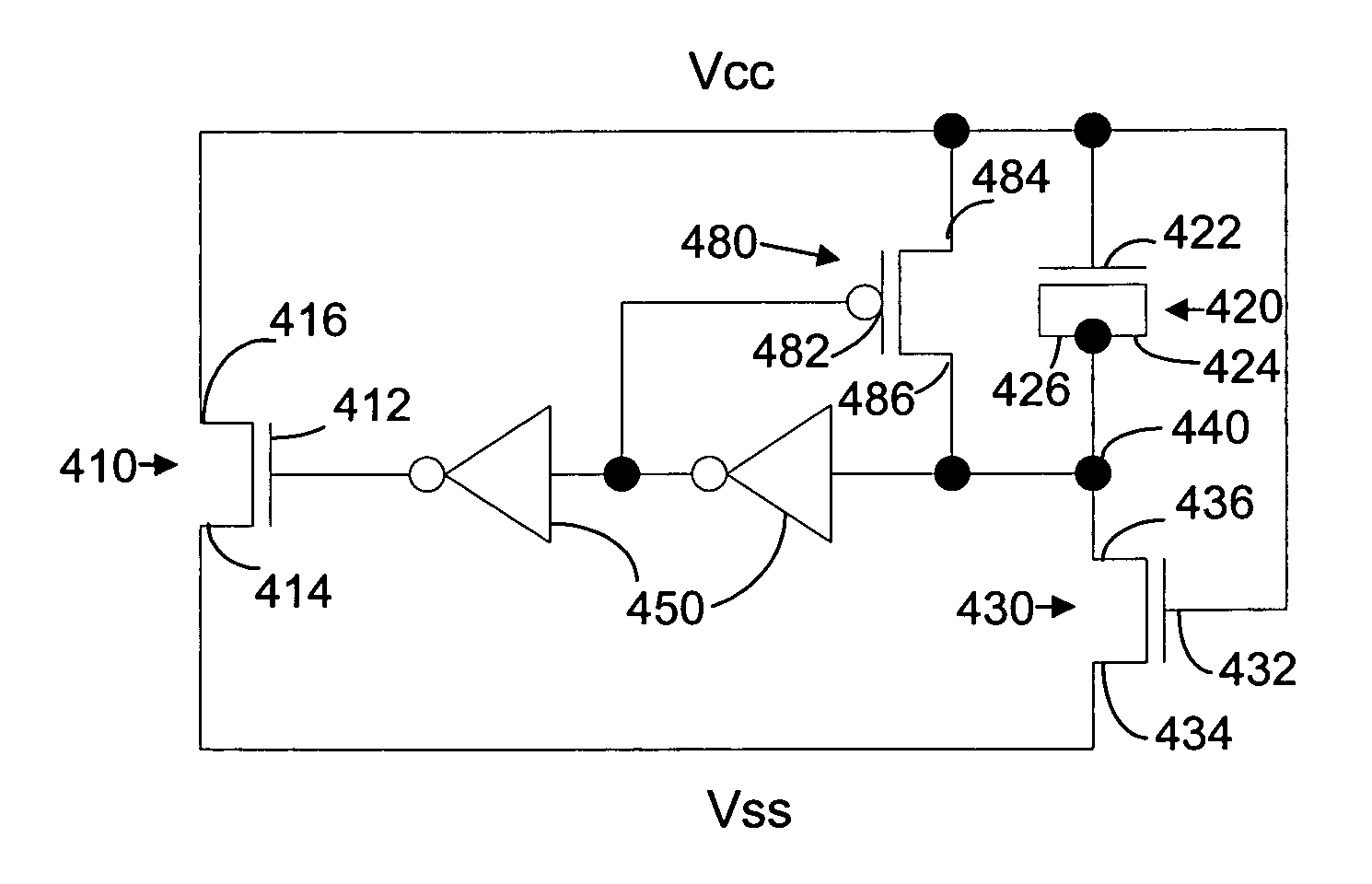
The present invention is a clamp circuit that includes a low voltage, thin oxide MOS transistor and a trigger element. The trigger element includes a timing element and at least one inverter. The source and drain of the MOS transistor are connected between a first node and a second node. The timing element includes a capacitive element and a resistive element connected between the first and second nodes. The inverter is connected between the gate of the MOS transistor and a third node between the capacitive element and the resistive element. The capacitive element and resistive element can be implemented in low voltage, thin oxide MOS transistors. The technical effect of this invention is to provide a clamp circuit that can effectively control the voltage levels of a circuit, and to provide a flexible and efficient way to trigger the circuit.

Problems solved by technology

This large spacing, however, leads to a large layout area for this structure.
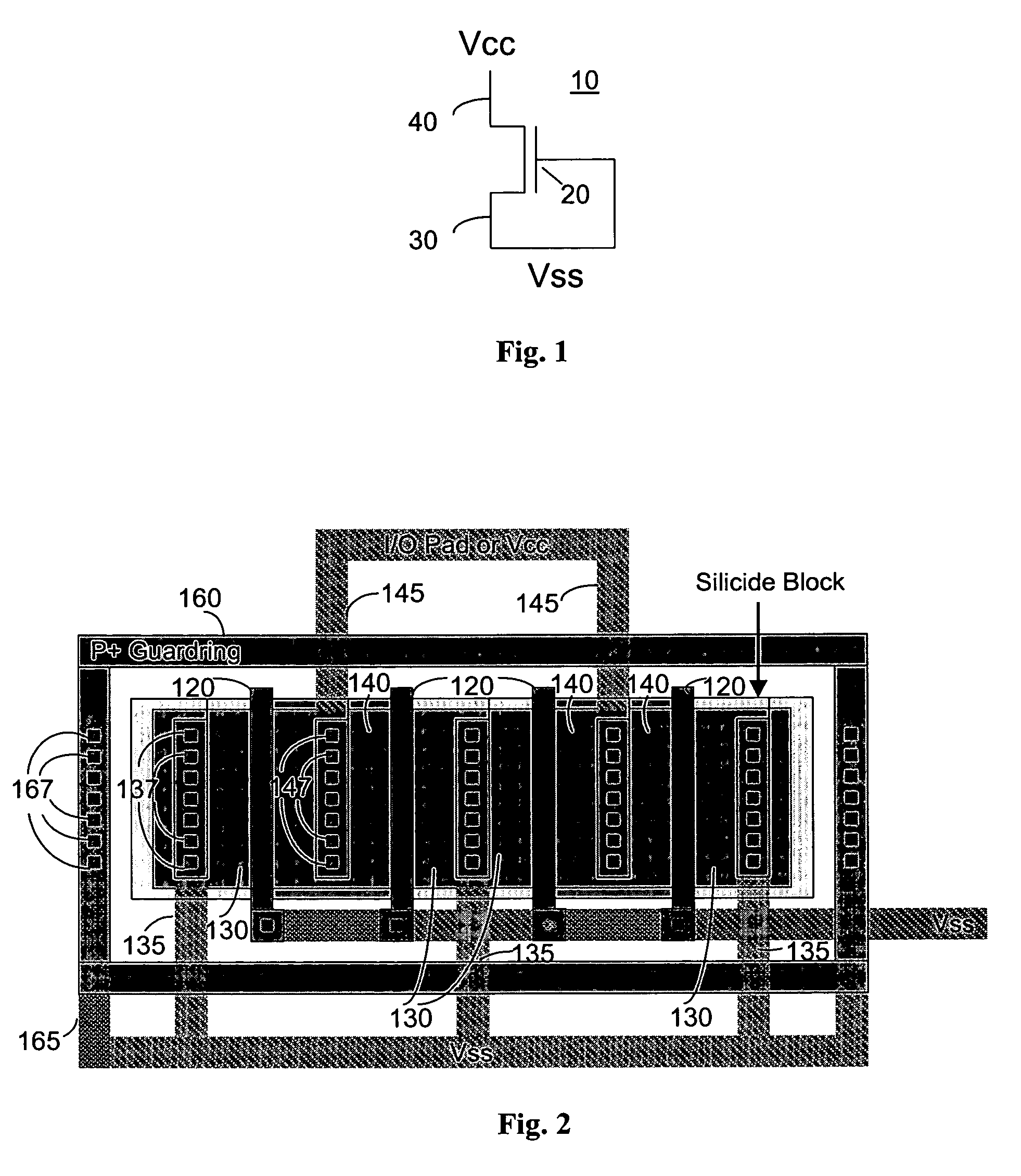
The problems with the grounded gate NMOS ESD power clamp such as that shown in FIGS. 1 and 2 are:a) The large space between the source and drain contacts and the gate results in a large structure area for the silicide block layout approach.b) It is difficult to guarantee that the ESD power clamp will turn on before other devices connected between Vcc and Vss are damaged.c) The above problem is exacerbated when the capacitance between Vcc and Vss is small.
This leads to a very fast ramp rate of the voltage between Vcc and Vss during an ESD event.
The problems with the non-breakdown alternative shown in FIG. 3 are:a) The width of the NMOS device must be very large to keep the transistor away from the snapback region.b) The trigger circuit must be tuned to work for a relatively narrow range of ESD voltage ramp rates on the Vcc bus.
Since the ESD voltage ramp rate is dependent on the total capacitance between Vcc and Vss, it may not be possible to guarantee that the structure will work for any possible capacitance.c) For a large enough capacitance between Vcc and Vss, the ramp rate of the voltage on Vcc during an ESD event may be the same or slower than the ramp rate when the circuit is being powered up during normal operation.

Method used


Image

  • Gate triggered ESD clamp
  • Gate triggered ESD clamp
  • Gate triggered ESD clamp

Examples


Embodiment Construction

[0027]The invention uses a non-breakdown approach to solve the problems with prior art devices. In a preferred embodiment of the invention shown in FIG. 4, circuit 400 uses a low-voltage, thin oxide transistor 410 for the main power clamp to achieve much better area efficiency and thin low-voltage, oxide transistors 420 and 430 to provide the capacitive and resistive elements in a timing circuit for a trigger circuit. This arrangement enables triggering in response to both fast and slow voltage ramps. More specifically, circuit 400 comprises first, second and third thin oxide transistors 410, 420, 430, each having a gate 412, 422, 432 a source 414, 424, 434, and a drain 416, 426, 436. The source and drain of transistor 410 are connected between a first node and a second node. Illustratively, the first node is at Vcc, which is the power supply voltage, and the second node is at Vss, which is ground. The source 424 and drain 426 of transistor 420 are connected together so that transis...


PUM


Abstract

The clamp circuit of the present invention comprises a low voltage, thin oxide MOS transistor and a trigger element comprising a timing element and at least one inverter. The source and drain of the MOS transistor are connected between a first node and a second node. The timing element comprises a capacitive element and a resistive element connected between the first and second nodes. The inverter is connected between a third node between the capacitive element and the resistive element and the gate of the MOS transistor. Advantageously, one or both of the capacitive element and the resistive element is also implemented in low voltage, thin oxide MOS transistors.

Description

BACKGROUND OF THE INVENTION[0001]A grounded gate NMOS transistor 10 shown in FIG. 1 is commonly used as a power supply electrostatic discharge (ESD) clamp. NMOS transistor 10 comprises a gate 20, a source 30, and a drain 40. Gate 20 and source 30 are coupled together and connected to ground, Vss. Drain 40 is normally connected to a power supply voltage, Vcc. This device provides ESD protection by switching to the low-impedance “snapback” regime when a large enough voltage appears between Vcc and Vss to cause the drain junction to break down.[0002]The NMOS device is usually implemented as a multi-finger transistor. FIG. 2 shows a layout style used with a self-aligned silicide (salicide) process to provide acceptable ESD performance. The layout of FIG. 2 comprises a gate 120, source diffusions 130, source leads 135, drain diffusions 140, and drain leads 145. Following known practice, the source and drain diffusions 130, 140 are clad in a metal silicide (not shown) to reduce the contac...

Claims


Application Information

Patent Timeline
Patent Type & Authority Patents(United States)
IPC IPC(8): H03K5/08H03L5/00H01L27/02H02H9/04
CPCH01L27/0285H01L27/0274
Inventor WATT, JEFFREY
Owner ALTERA CORP
Features
  • R&D
  • Intellectual Property
  • Life Sciences
  • Materials
  • Tech Scout
  • Unparalleled Data Quality
  • Higher Quality Content
  • 60% Fewer Hallucinations
Learn More