Integrated CMOS imaging array dark current monitor

a technology monitor, which is applied in the field of digital imaging, can solve the problems of not accounted for “dark current” in the prior art of cmos image array, ccd arrays have a longer history and much more time to solve problems,

Inactive Publication Date: 2006-09-05
MELA SCIENCES
View PDF24 Cites 36 Cited by
  • Summary
  • Abstract
  • Description
  • Claims
  • Application Information

AI Technical Summary

Problems solved by technology

CCD arrays have a longer history and much more time to solve problems arising in manufacture and use.
The prior art of CMOS image arrays is deficient in that the “dark current” is not accounted for in the case that the array temperature, and also the variation in temperature over the array, changes with time.
For the case of a CMOS integrated circuit application, where many functions are carried out on a monolithic semiconductor chip, this is a serious deficiency.
The temperature and variation in temperature may change as the device is used for imaging, so that the dark current contribution to the image is variable and unaccounted for.

Method used


Image

  • Integrated CMOS imaging array dark current monitor
  • Integrated CMOS imaging array dark current monitor
  • Integrated CMOS imaging array dark current monitor

Examples


Embodiment Construction

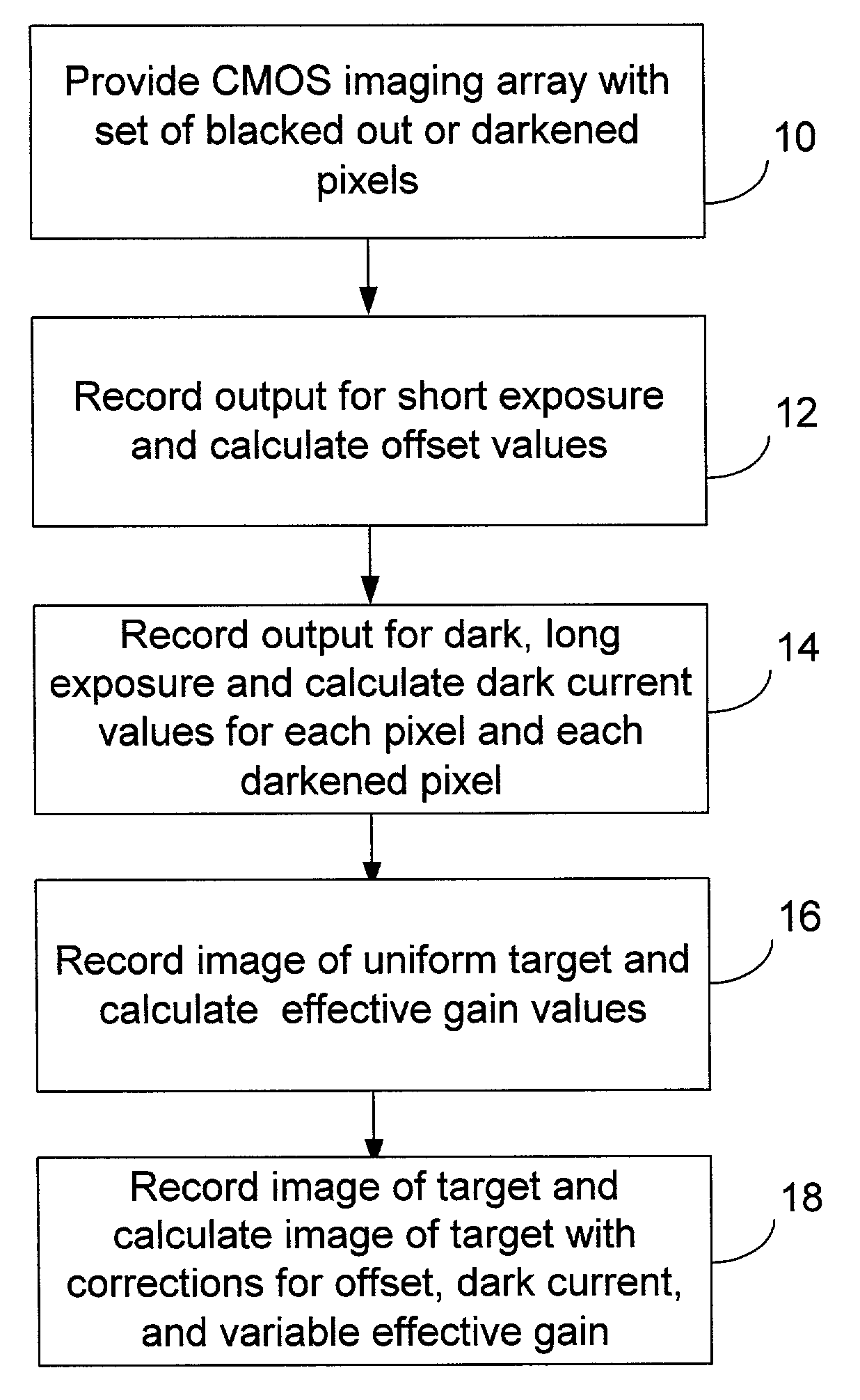
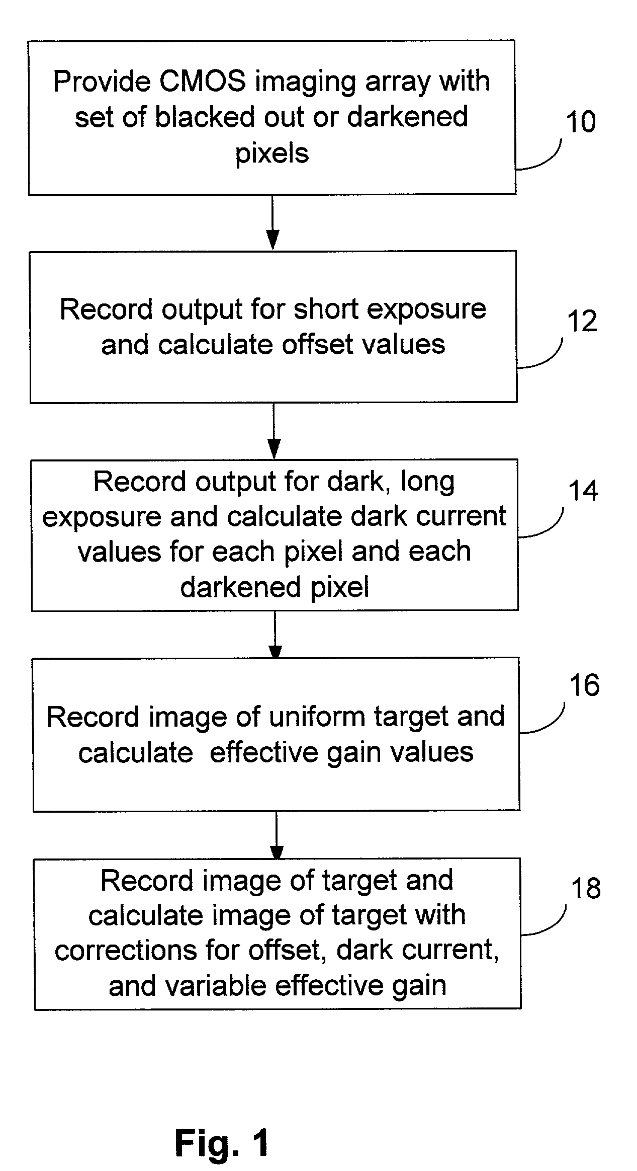
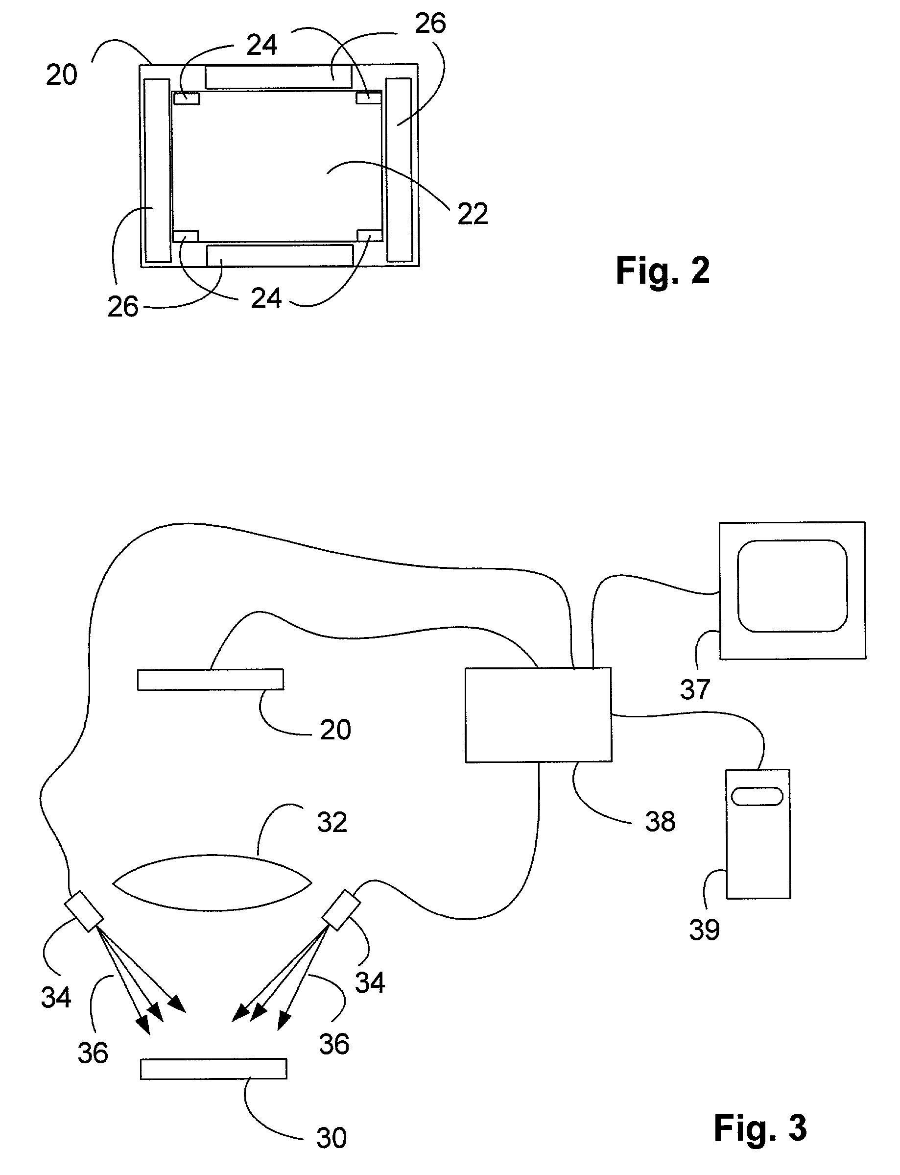
[0014]To achieve repeatability of performance of an imaging system, it is necessary to compensate for or remove sensor and illumination artifacts in the system. In critical applications, such as imaging of biological tissue for diagnosis of such diseases as cancer, the performance of the imaging system is critical. The imaging system is made up of an illumination system for illuminating an object, an optical system for projecting an image of the object on to an image detector, and hardware and software for producing a computer and / or human readable output for further evaluation. Our purpose in imaging an object is to quantify the amount of light emitted at each point on the target, so as to most accurately map the radiant emittance from each point on the object. For purposes of the following discussion, we make the simplifying assumption, which need not be true, that transillumination and multiple-scattering effects are sufficiently small that all of the light emitted can be conside...


PUM


Abstract

A method, apparatus, and system for accounting for dark current in the output of an imaging array is presented. A dark current monitor on the monolithic semiconductor imaging array is provided. The dark current monitor may be darkened pixels of the imaging array, darkened pixels of another array, or a temperature monitor and associated circuitry necessary to calculate relative dark current from the monitored temperature.

Description

FIELD OF THE INVENTION[0001]The field of the invention is the field of digital imaging using complementary metal oxide semiconductor (CMOS) technology.BACKGROUND OF THE INVENTION[0002]Modern imaging systems using charged coupled device (CCD) arrays and complementary metal oxide semiconductor CMOS arrays have come into increasing use for both industrial and consumer applications. CCD arrays have a longer history and much more time to solve problems arising in manufacture and use. CCD arrays have fewer dark current problems than CMOS arrays. However, CMOS arrays promise less expensive imaging, principally because other functions may be combined on the semiconductor substrate and the well honed techniques developed for computer technology may be used to produce the arrays.[0003]Prior art CMOS arrays have an array of pixels arranged in rows and columns, where light is absorbed in the semiconductor substrate to generate electrons, and the electrons are stored until they are “read out” to...

Claims


Application Information

Patent Timeline
Patent Type & Authority Patents(United States)
IPC IPC(8): H04N5/217H04N5/361H04N5/374
CPCH04N5/361H04N25/63
Inventor JACOBS, ADAM
Owner MELA SCIENCES
Why Eureka
Try Eureka