SRAM cell structure and circuits

a cell structure and circuit technology, applied in the field of static random access memory circuits, can solve the problems of large portion of the total power consumption of the device, large current level cannot be ignored, and power consumption is a trade-off between read speed and power consumption, so as to reduce leakage currents, increase memory speed, and read high speed

Inactive Publication Date: 2006-09-05
ZMOS TECH
View PDF8 Cites 15 Cited by
  • Summary
  • Abstract
  • Description
  • Claims
  • Application Information

AI Technical Summary

Benefits of technology

[0016]A static random access memory (SRAM) circuit is described which provides reduced leakage currents and high reading speed. The novel architecture described is configured with a novel read sensing structure that can be utilized in combination with differing voltage thresholds for different functional blocks within the device. These aspects of the invention can be utilized separately or in combinations to increase the speed of memory. and / or to lower the power dissipation, such as resulting from the leakage currents.
[0021]The invention may also be described in terms of a method of accessing cells of a static memory, comprising: (a) maintaining data written to transistors forming a data latch for a static memory cell; (b) applying a read word signals to activate read word transistors; and (c) sensing the output of the read word transistors in a sense amplifier coupled between bit lines to generate a data bit output. Furthermore, functional blocks within the static memory can be configured with lower voltage thresholds, such as the read block, or the read and write blocks, wherein faster speeds and lower leakage currents can be exhibited by the circuit.
[0026]Another aspect of the invention is an SRAM cell structure in which one terminal of read path transistors are connected together with one terminal of alternating read path transistors and to a virtual node which is connected to a source transistor to suppress leakage current of cell blocks.

Problems solved by technology

However, there is a trade-off between power consumption and read speed.
However, with regard to more advanced technology such as 0.13 μm technology, since this current is then on the order of tens of nA (10e−9), the level of current can no longer be ignored.
This level of leakage current equates to a large portion of the total power consumption for the device.
Therefore, the power consumption component which arises as a result of cell leakage current becomes quite substantial.
As the systems relying on SRAM become increasingly complex, the density of SRAM will continue to increase, and the total power consumed by cell leakage currents based on conventional SRAM architectures will continue to increase.
However, when these cell access transistors and cell pull-down transistors increase in size, leakage currents flowing through these transistors also increase.
Therefore, a trade-off between the cell leakage current and the cell read time makes SRAM design complicated and difficult as the operating voltage goes down.
However, due to a drastic increase of the cell leakage current, the conventional 6T SRAM cell structure is facing a technical barrier to meet the design requirement.
When device sizes increase and the threshold voltage of transistors decreases to meet the required speed, the power consumption due to the cell leakage current is a concern.
When device sizes are scaled down and the threshold voltage of transistors increases to suppress leakage current, the cell read speed is degraded due to reduced current driving capability of the cell access and pull-down transistors.

Method used


Image

  • SRAM cell structure and circuits
  • SRAM cell structure and circuits
  • SRAM cell structure and circuits

Examples


Embodiment Construction

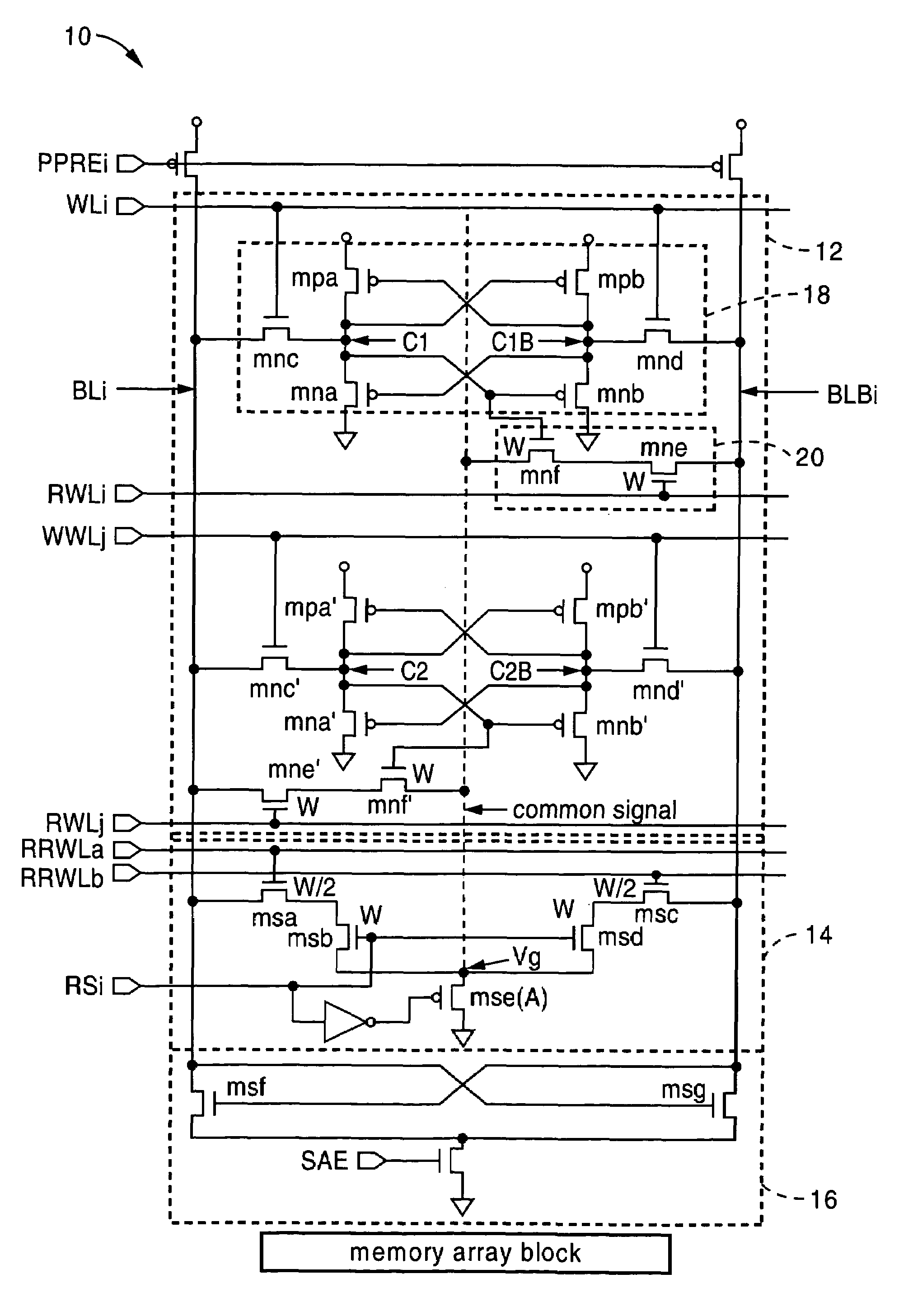
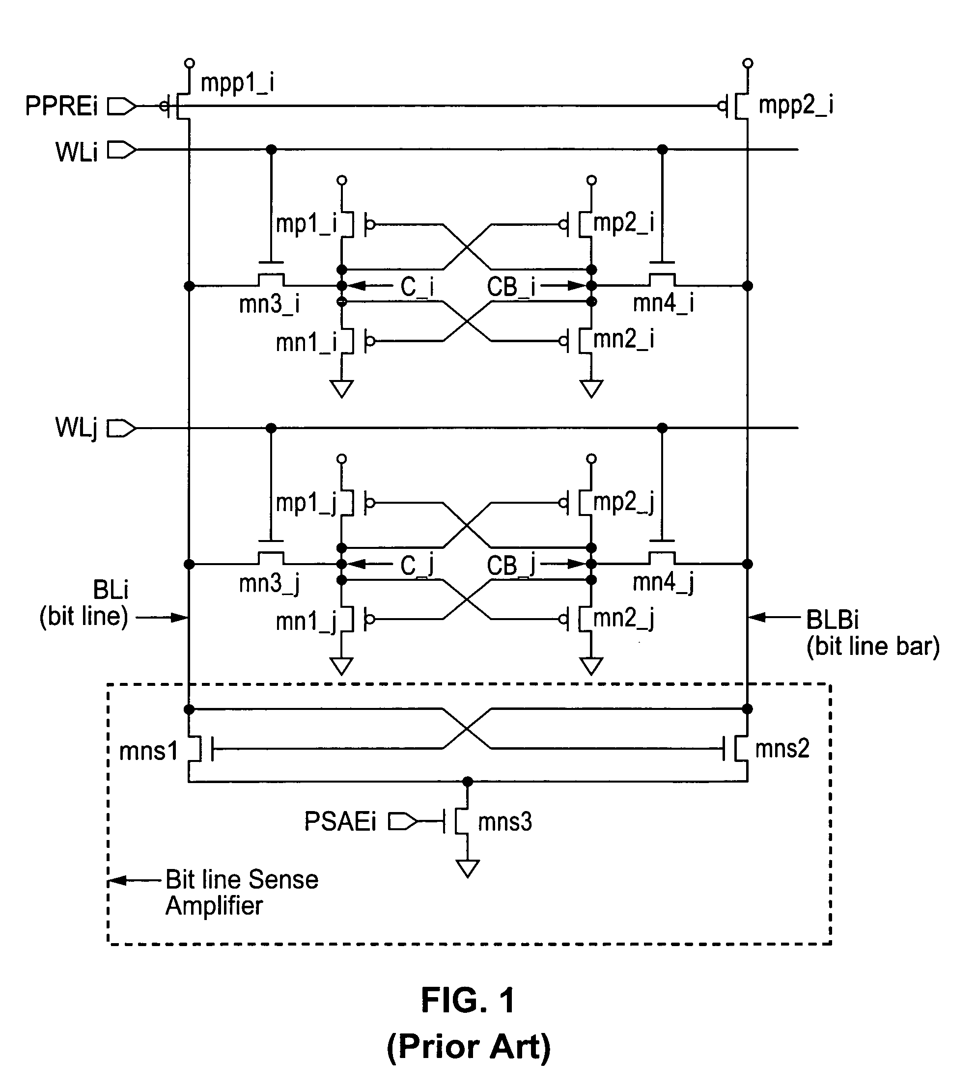
[0042]Referring more specifically to the drawings, for illustrative purposes the present invention is embodied in the apparatus generally shown in FIG. 3 through FIG. 6. It will be appreciated that the apparatus may vary as to configuration and as to details of the parts, and that the method may vary as to the specific steps and sequence, without departing from the basic concepts as disclosed herein.

[0043]The new SRAM cell structure and related sensing scheme are configured for overcoming a number of the problems which arise with conventional SRAM architectures. One improvement is an architecture in which specific functional blocks can be designed with different threshold voltages to control leakage. For example, the transistors of the read circuit being configured with a lower voltage threshold than the storage transistors. As a second example, the write circuit is configured with a lower voltage threshold than the storage transistors, and the transistors of the read circuit are co...


PUM


Abstract

An SRAM circuit structure and method for reducing leakage currents and / or increasing the speed of the devices. Various forms of SRAM devices may be fabricated utilizing the techniques, such as single port and dual port RAM devices. By way of example the SRAM structure utilizes separate write and read lines, splits the circuit into portions which can benefit from having differing threshold levels, and can allow splitting read path transistors for connection to a first terminal and a virtual node connected to a source transistor. The structure is particularly well suited for forming transistors in a combination of NMOS and PMOS, or solely in NMOS. Memory arrays may be organized according to the invention in a number of different distributed or lumped arrangements with the reference read paths and sense blocks being either shared or dedicated.

Description

CROSS-REFERENCE TO RELATED APPLICATIONS[0001]This application claims priority from U.S. provisional application Ser. No. 60 / 484,565 filed on Jul. 1, 2003, incorporated herein by reference in its entirety.STATEMENT REGARDING FEDERALLY SPONSORED RESEARCH OR DEVELOPMENT[0002]Not ApplicableINCORPORATION-BY-REFERENCE OF MATERIAL SUBMITTED ON A COMPACT DISC[0003]Not ApplicableNOTICE OF MATERIAL SUBJECT TO COPYRIGHT PROTECTION[0004]A portion of the material in this patent document is subject to copyright protection under the copyright laws of the United States and of other countries. The owner of the copyright rights has no objection to the facsimile reproduction by anyone of the patent document or the patent disclosure, as it appears in the United States Patent and Trademark Office publicly available file or records, but otherwise reserves all copyright rights whatsoever. The copyright owner does not hereby waive any of its rights to have this patent document maintained in secrecy, includ...

Claims


Application Information

Patent Timeline
Patent Type & Authority Patents(United States)
IPC IPC(8): G11C11/00G11CG11C11/413G11C11/419
CPCG11C11/419G11C11/413
Inventor SOHN, JEONG-DUK
Owner ZMOS TECH
Why Eureka
Try Eureka