Protection circuit section for semiconductor circuit system

Inactive Publication Date: 2006-09-12
KK TOSHIBA
View PDF12 Cites 27 Cited by
  • Summary
  • Abstract
  • Description
  • Claims
  • Application Information

AI Technical Summary

Benefits of technology

[0061]FIG. 19 is an equivalent circuit diagram of another conventional ESD prote

Problems solved by technology

However, if the voltage applied to the LVTSCR2, which is higher than a snap-back breakdown voltage, is higher than the gate breakdown voltage of the N

Method used


Image

  • Protection circuit section for semiconductor circuit system
  • Protection circuit section for semiconductor circuit system
  • Protection circuit section for semiconductor circuit system

Examples


first embodiment

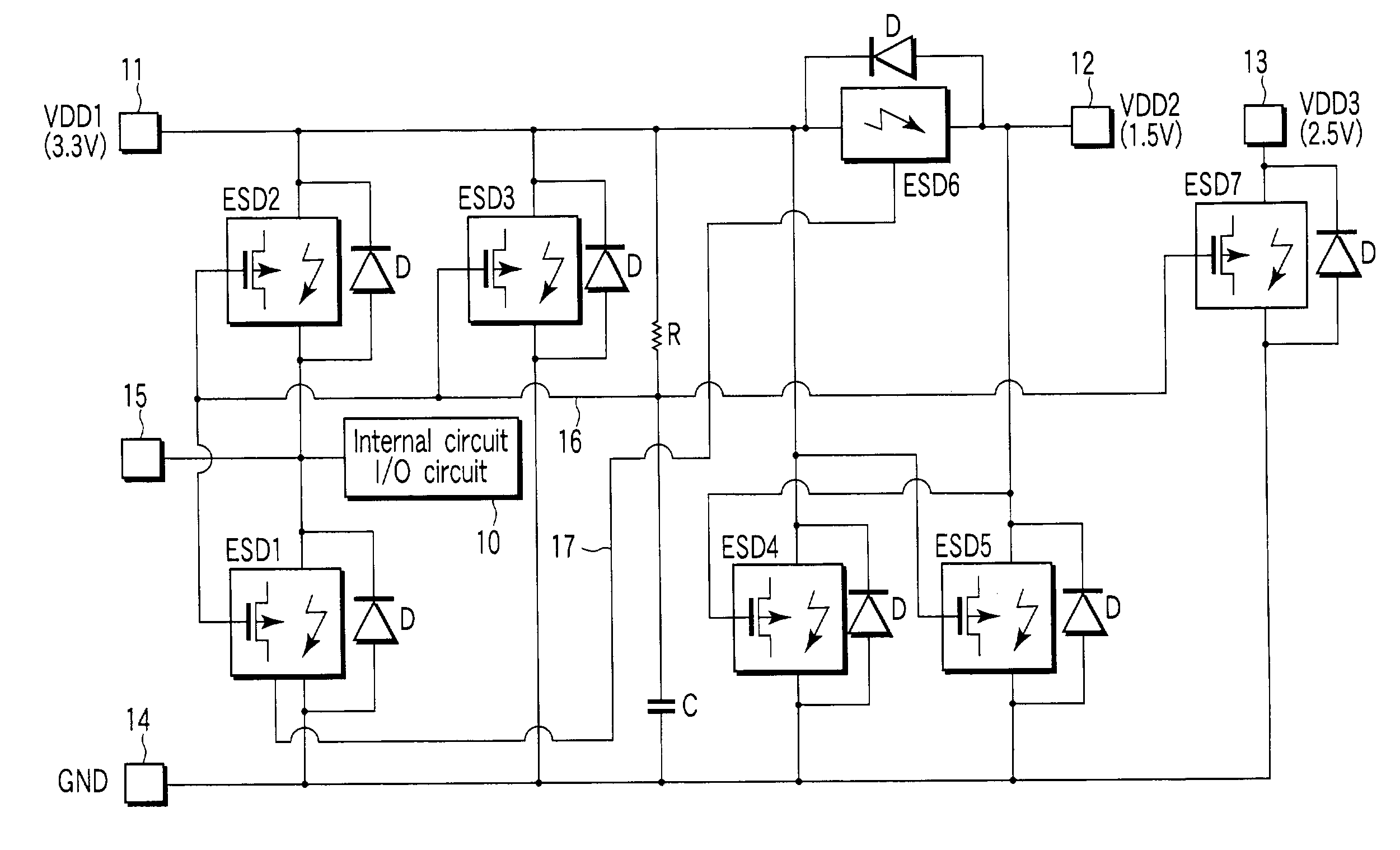
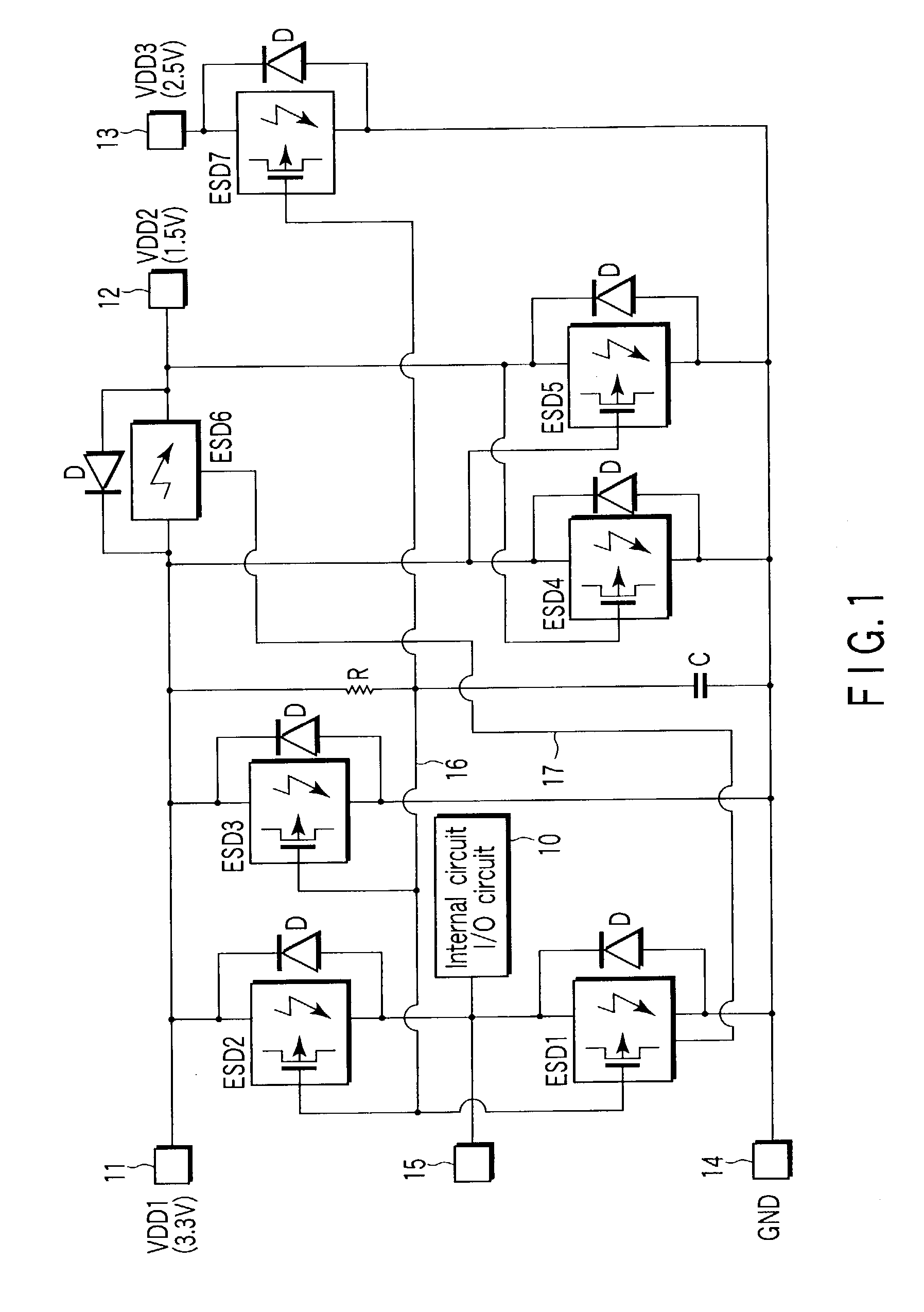
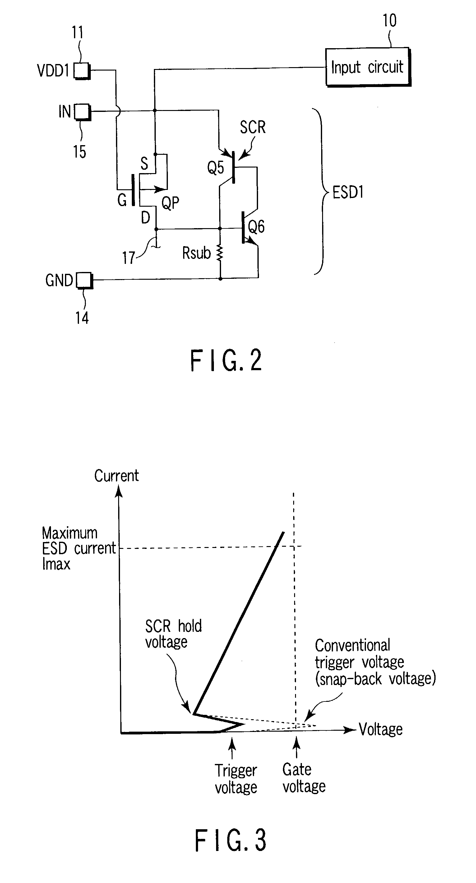
[0079]FIG. 2 is an equivalent circuit diagram showing a protection circuit section according to an embodiment of the present invention, which corresponds to the first ESD protection circuit ESD1 shown in FIG. 1. As described, a VDD1 pad 11, input pad 15, and GND pad 14 are pads electrically separated from each other.

[0080]The protection circuit section shown in FIG. 2 has an SCR for ESD protection, whose current passage between the anode and cathode is connected between the input pad 15, which is connected to, e.g., the input circuit 10 of an CMOS-LSI, and the GND pad 14. The SCR includes a PNP transistor Q5 and NPN transistor Q6 combined to equivalently form a thyristor. Specifically, the base and collector of the PNP transistor Q5 are connected to the collector and base of the NPN transistor Q6, respectively. The emitter of the PNP transistor Q5 comes to the anode, and the emitter of the NPN transistor Q6 comes to the cathode. A substrate resistance Rsub exists between the base of...

second embodiment

[0120]ESD protection circuits may be utilized not only to protect an input circuit or output circuit, but also to clamp the potential between power supplies to protect a current itself between the power supplies. As an example of this concept, an explanation will be given of a second embodiment in which a plurality of power supply routes are respectively provided with ESD protection circuits in a CMOS-LSI.

[0121]FIG. 9 is an equivalent circuit diagram showing the fourth ESD protection circuit ESD4 and the fifth ESD protection circuit ESD5 along with diodes for allowing a current to flow in the reverse direction, which are shown in FIG. 1. As shown in FIG. 9, the fourth ESD protection circuit ESD4 and a diode combination for allowing a current to flow in the reverse direction is connected between a VDD1 pad 11 and GND pad 14. Similarly, the fifth ESD protection circuit ESD5 and a diode combination for allowing a current to flow in the reverse direction is connected between a VDD2 pad ...

third embodiment

[0124]FIG. 10 is an equivalent circuit diagram showing the third ESD protection circuit ESD3, the seventh ESD protection circuit ESD7, and its trigger bias circuit, along with diodes for allowing a current to flow in the reverse direction, which are shown in FIG. 1.

[0125]As shown in FIG. 10, the gate of the PMOS transistor QP for inputting a trigger, provided in each of these ESD protection circuits is connected to the output node of an RC integrator circuit through a trigger bias line 16. The RC integrator circuit is arranged such that a resistance element R and capacitance element C are connected in series between the highest potential power supply pad (VDD1 pad 11) and GND pad 14.

[0126]In the arrangement described above, when an inputted surge voltage has to be handled by the ESD protection circuit, the trigger bias line 16 is set at GND. When the VDD1 pad 11 receives a positive surge voltage in this state, if a forward bias larger in absolute value than its own gate threshold vo...


PUM


Abstract

A semiconductor circuit system has first, second, and third external terminals electrically separated from each other. The first external terminal is configured to receive a first power supply voltage in a normal operation. A protection circuit section is provided in the circuit system and includes a rectifier to allow a surge current to pass therethrough. The rectifier has a current passage connected between a specific terminal connected to a protection target and the third external terminal. The protection circuit section further includes a first PMOS transistor configured to trigger the rectifier, based on a surge voltage inputted into the second external terminal. The first PMOS transistor has a current passage connected between the second external terminal and a base of the NPN transistor. The first PMOS transistor has a gate connected to the first external terminal.

Description

CROSS-REFERENCE TO RELATED APPLICATIONS[0001]This application is based upon and claims the benefit of priority from the prior Japanese Patent Application No. 2002-118253, filed Apr. 19, 2002, the entire contents of which are incorporated herein by reference.BACKGROUND OF THE INVENTION[0002]1. Field of the Invention[0003]The present invention relates to a protection circuit section for protecting a protection target in a semiconductor circuit system from a surge. Typically, the protection circuit section employs a silicon controlled rectifier (SCR) to protect a protection target from electro-static discharge (ESD). For example, the protection circuit section is applied to a CMOS-LSI of the low power supply voltage type.[0004]2. Description of the Related Art[0005]There is a known technique in which an ESD protection circuit is connected to the input circuit or output circuit of a CMOS-LSI to protect it from ESD breakdown. The ESD protection circuit employs a protection element, such ...

Claims


Application Information

Patent Timeline
IPC IPC(8): H02H9/00H01L29/74H01L21/822H01L21/8238H01L27/02H01L27/04H01L27/06H01L27/08H01L27/092
CPCH01L27/0251G11C11/40
Inventor KITAGAWA, NOBUTAKA
Owner KK TOSHIBA
Why Eureka
Try Eureka