Semiconductor Device

a technology of semiconductor devices and resistors, applied in relays, emergency protective arrangements for limiting excess voltage/current, pulse techniques, etc., can solve problems such as great burden, and achieve the effects of reducing the variation rate of collector current, reducing the resistance value of resistance circuits, and reducing the switching element's turning off speed

Active Publication Date: 2013-06-20
FUJI ELECTRIC CO LTD
View PDF12 Cites 26 Cited by
  • Summary
  • Abstract
  • Description
  • Claims
  • Application Information

AI Technical Summary

Benefits of technology

[0019]Preferably, a semiconductor device of the invention increases the resistance value of the resistance circuit by operating so as to change a connection condition of a plurality of resistors.
[0020]In a semiconductor device of the invention, the gate resistance is changed to increase the gate resistance value for the switching element, for example, based on the collector voltage and the ON time at one cycle before, of the semiconductor switching element. As a result, the turning-OFF speed of the switching element is slowed down, decreasing the variation rate of the collector current. Thus, the surge voltage at the turning OFF is reduced.
[0021]Therefore, the voltage applied between the collector and the emitter of the switching element is reduced, which suppresses the self-heating of the switching element and mitigates the burden on the switching element and the gate control circuit.

Problems solved by technology

Although these conventional technologies can avoid electrical breakdown due to overvoltage, the self-heating abruptly increases at the turn OFF time presenting a problem of great burden on the switching element 1 and a gate control circuit for it.

Method used


Image

  • Semiconductor Device
  • Semiconductor Device
  • Semiconductor Device

Examples


Embodiment Construction

[0026]A preferred embodiment according to the present invention will be described in the following with reference to the accompanying drawings.

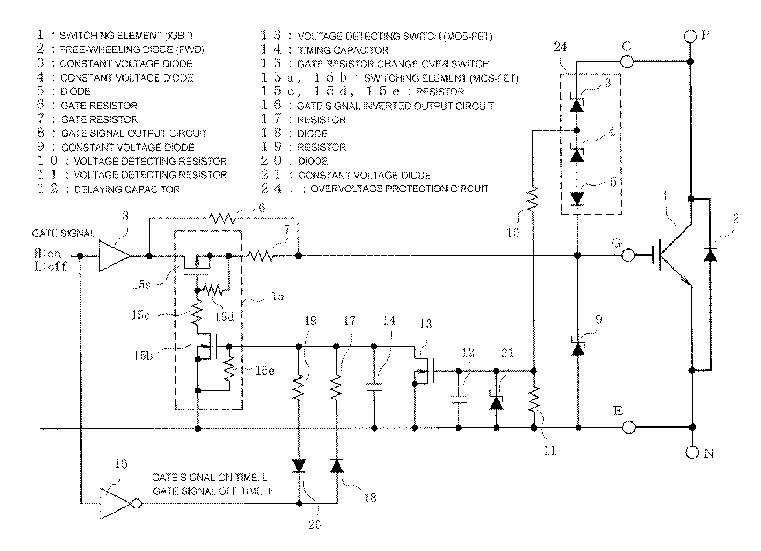
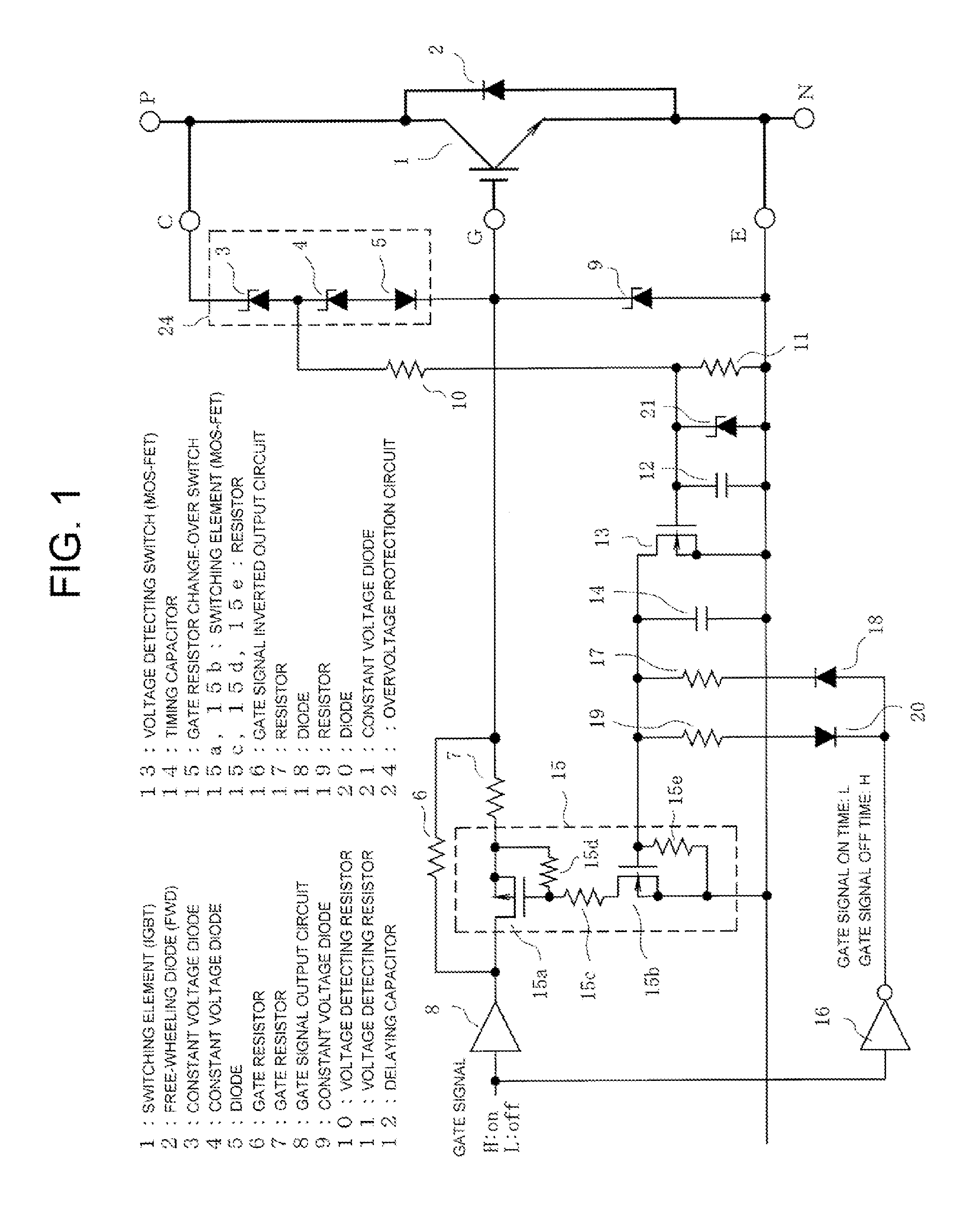
[0027]Referring to FIG. 1, the reference numeral 1 designates a semiconductor switching element such as an IGBT; the symbol C designates a collector terminal connected to the positive terminal P of a DC power supply; G, the gate terminal of the switching element 1; E, an emitter terminal connected to the negative terminal N of the DC power supply; and the reference numeral 2 designates a free-wheeling diode.

[0028]The gate terminal G corresponds to, for example, a “control terminal,” and the collector terminal C and the emitter terminal E correspond to, for example, “output terminals.”

[0029]Between the connected collector terminal C and gate terminal G is a series-connected circuit of constant voltage diodes 3, 4 and a reverse blocking diode 5 for blocking a reverse gate current. A constant voltage diode 9 is connected between the gate termina...


PUM


Abstract

In a semiconductor device, a surge voltage is lowered on turning OFF of a switching element, and output current is reduced on turning ON of the switching element in a non-saturated condition to achieve a reduced amount of self-heating. The semiconductor device can comprise a semiconductor switching element, an overvoltage protection circuit, and a resistance circuit to transmit a control signal for turning the switching element ON and OFF to a control terminal of the switching element. The semiconductor device can further comprise a voltage detecting switch that receives a signal corresponding to a voltage appearing at the output terminal of the switching element on turning OFF of the switching element, and a gate resistor change-over switch that operates according to a voltage of a timing capacitor connected to the output side of the voltage detecting switch to increase a resistance value of the resistance circuit.

Description

CROSS-REFERENCE TO RELATED APPLICATION[0001]This application is based on, and claims priority to, Japanese Patent Application No. 2011-272874, filed on Dec. 14, 2011, contents of which are incorporated herein by reference.BACKGROUND OF THE INVENTION[0002]1. Field of the Invention[0003]The present invention relates to a semiconductor device providing an overvoltage protection function for a switching element.[0004]2. Description of the Related Art[0005]FIG. 4 shows a conventional example of a semiconductor device providing an overvoltage protection function for a switching element.[0006]In FIG. 4, the reference numeral 1 designates a semiconductor switching element, for example, an insulated gate bipolar transistor (IGBT) and the reference numeral 2 designates a free-wheeling diode (FWD). Between the collector C and the gate G of the switching element 1 is connected an overvoltage protection circuit 23 composed of a series-connected circuit of a constant voltage diode 3 and a reverse...

Claims


Application Information

Patent Timeline
Patent Type & Authority Applications(United States)
IPC IPC(8): H02H3/20H01H47/00
CPCH02H3/20H03K17/166H03K17/0828H01H47/00
Inventor TAKEUCHI, TORU
Owner FUJI ELECTRIC CO LTD
Why Eureka
Try Eureka