Growth method of light-emitting diode (LED) epitaxial wafer

A technology of LED epitaxial wafers and growth methods, which is applied in the direction of electrical components, circuits, semiconductor devices, etc., can solve the problems of uneven current distribution of epitaxial layers, high chip voltage, and current congestion, etc., to achieve enhanced electronic horizontal expansion capabilities and save consumption , The effect of reducing the driving voltage

Active Publication Date: 2013-05-15
XIANGNENG HUALEI OPTOELECTRONICS
View PDF4 Cites 16 Cited by
  • Summary
  • Abstract
  • Description
  • Claims
  • Application Information

AI Technical Summary

Problems solved by technology

Moreover, the traditionally grown N-type GaN layer, because the doped Si concentration is the same, the resistance value of each place is the same
This makes the electron transportation process choose the shortest path for transmission, and there will be a phenomenon of current congestion on the shortest path
At the same time, the current distribution of the entire epitaxial layer is uneven, and the current flowing through the quantum well is relatively concentrated. As a result, the voltage of the chip is high and the light efficiency is low.

Method used


Image

  • Growth method of light-emitting diode (LED) epitaxial wafer
  • Growth method of light-emitting diode (LED) epitaxial wafer
  • Growth method of light-emitting diode (LED) epitaxial wafer

Examples


Embodiment approach 1

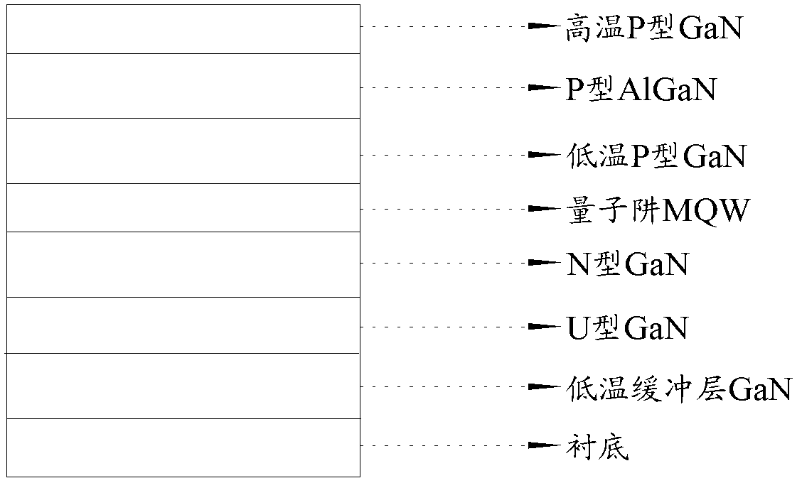
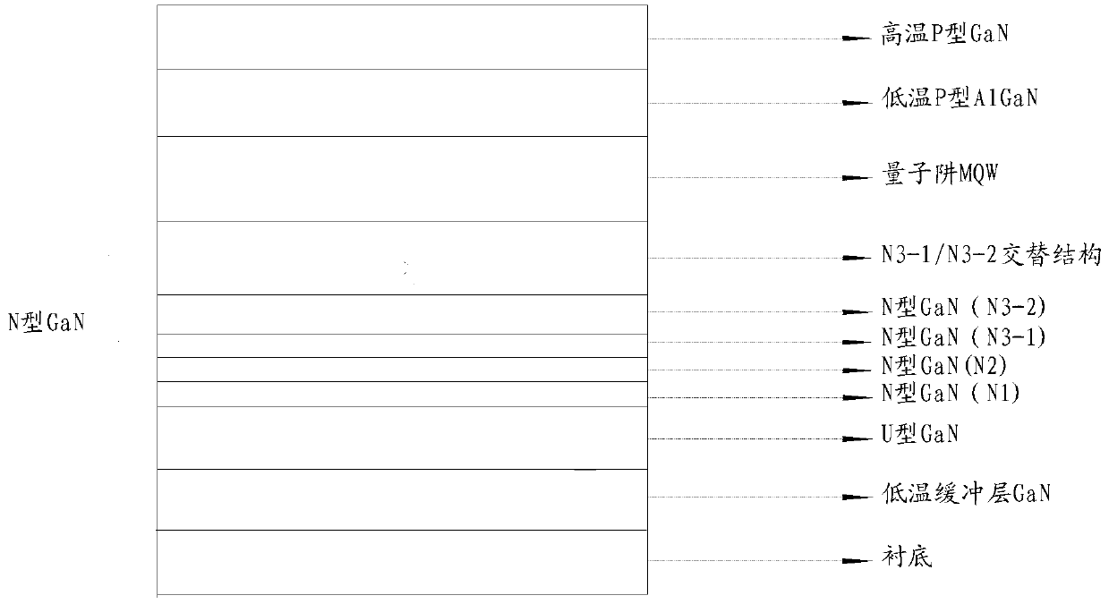
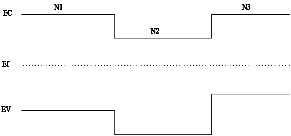
[0055] Sample 1 was prepared according to the traditional LED growth method, and sample 2 was prepared according to the method described in the present invention. The difference between sample 1 and sample 2 epitaxial growth method parameters is that sample 2 uses 16 alternate structural layers consisting of N3-1 layer and N3-2 layer alternately grown to replace the N3 layer grown in sample 1. For details, please refer to Table 1 . Sample 1 and sample 2 were plated with 200nm of ITO layer under the same pre-process conditions, 130nm of Cr / Pt / Au electrodes were plated under the same conditions, and the protective layer of SiO was plated under the same conditions. 2 About 50nm, and then grind and cut the sample into chip particles of 762μm×762μm (30mi×30mil) under the same conditions, and then select 150 crystal grains at the same position for sample 1 and sample 2, and package them under the same packaging process. into a white LED. Then an integrating sphere was used to test...

Embodiment approach 2

[0060] Sample 3 was prepared according to the traditional LED growth method, and sample 4 was prepared according to the method described in the present invention. The difference between sample 3 and sample 4 in epitaxial growth method parameters is that sample 4 uses 15 alternate structural layers formed by alternate growth of N3-1 layer and N3-2 layer instead of the N3 layer grown in sample 3. For details, please refer to Table 2 . Samples 3 and 4 were plated with 180nm of ITO layer under the same pre-process conditions, 120nm of Cr / Pt / Au electrodes were plated under the same conditions, and the protective layer of SiO was plated under the same conditions. 2 About 50nm, and then grind and cut the sample into chip particles of 250μm×457μm (10mi×18mil) under the same conditions, and then select 150 crystal grains at the same position for sample 3 and sample 4, and package them under the same packaging process. into a white LED. Then an integrating sphere was used to test the ...


PUM


Abstract

Disclosed is a growth method of a light-emitting diode (LED) epitaxial wafer. When growth of an N type doped gallium nitride (GaN) layer with silicon (Si) is carried out, a method of alternate growth of the N type doped GaN layer with Si and a U type undoped GaN layer with no Si is adopted. According to the growth method of the LED epitaxial wafer, the thickness of an original N type GaN layer is kept, a doped GaN layer with Si with continuous growth in a traditional growth method is modified into an alternate structure layer formed by the N type doped GaN layer with Si and a U type GaN layer with no doped Si, and usage amount of dopant is saved to a certain degree. In an alternate structure of the N type doped GaN layer with Si and the U type undoped GaN layer with no Si, the doped GaN lay with Si is low in resistance value, and the undoped GaN layer with no Si is high in resistance value. Due to the facts that the doped GaN layer with Si is low in resistance value, and the undoped GaN layer with no Si is high in resistance value, horizontal expansion capacity of electrons is strengthened, and thus a driving voltage is reduced, and meanwhile luminance and a lighting effect are improved.

Description

technical field [0001] The invention relates to a method for growing an LED epitaxial wafer. Background technique [0002] Semiconductor lighting technology is another revolution in lighting sources after incandescent lamps and fluorescent lamps. Semiconductor lighting technology has developed rapidly, has wide application fields, great energy-saving potential, and is green and environmentally friendly. It is recognized as one of the most promising high-tech energy-saving industries, and the core of semiconductor lighting is LED chips. The luminous efficiency of ordinary incandescent lamps is 15lm / W, while the luminous efficacy of LED lamps for lighting can reach more than 100lm / W, that is, a 6-watt LED lamp can replace a 40-watt incandescent lamp. LEDs have shown obvious energy-saving advantages in replacing traditional lighting. Continuously improving the luminous efficiency of LED lights, that is, reducing the voltage and increasing the luminous brightness at the rated d...

Claims


Application Information

Patent Timeline
Patent Type & Authority Applications(China)
IPC IPC(8): H01L33/14H01L33/00
Inventor 苗振林张宇牛凤娟
Owner XIANGNENG HUALEI OPTOELECTRONICS
Why Eureka
Try Eureka