Optical signal receiving circuit and optical signal receiving apparatus

a technology of optical signal and receiving circuit, applied in the direction of electromagnetic transmission, electromagnetic transceivers, transmission, etc., can solve the problems of output voltage amplitude and circuit operating limi

Inactive Publication Date: 2007-09-13
HITACHI LTD
View PDF2 Cites 16 Cited by
  • Summary
  • Abstract
  • Description
  • Claims
  • Application Information

AI Technical Summary

Benefits of technology

[0010]Referring to the circuit of FIG. 4, an increase in the resistance value of the feedback resistor 11 has a beneficial effect on improvement in the noise characteristic determining the minimum input sensitivity.
[0017]By use of a resistor as the current source in the differential circuit provided in the stage subsequent to the current-voltage converting circuit, it is made possible to lower the output voltage level of the current-voltage converting circuit, and thus realization of required dynamic range can be facilitated and the adverse effect on the bandwidth characteristic can be reduced.
[0021]A typical advantage obtained from the above means is that an optical signal receiving circuit and apparatus adapted operable with a single low voltage power supply can be realized.

Problems solved by technology

However, the output voltage amplitude of the trans-impedance amplifier 10 is given by input current amplitude multiplied resistance value of feedback resistor 11, and therefore, if the value of the feedback resistor 11 is increased, the output voltage amplitude becomes large, and this affects the operating limit of the circuit when a large signal is input thereto (this operating limit may hereinafter be called “overload limit.”) Accordingly, in order to keep a dynamic range of the circuit to satisfy the conditions for the demanded minimum input sensitivity and the overload limit, an issue arises how to suppress the effect of an increase in the value of the feedback resistor 11 on the overload limit.

Method used


Image

  • Optical signal receiving circuit and optical signal receiving apparatus
  • Optical signal receiving circuit and optical signal receiving apparatus
  • Optical signal receiving circuit and optical signal receiving apparatus

Examples


first embodiment

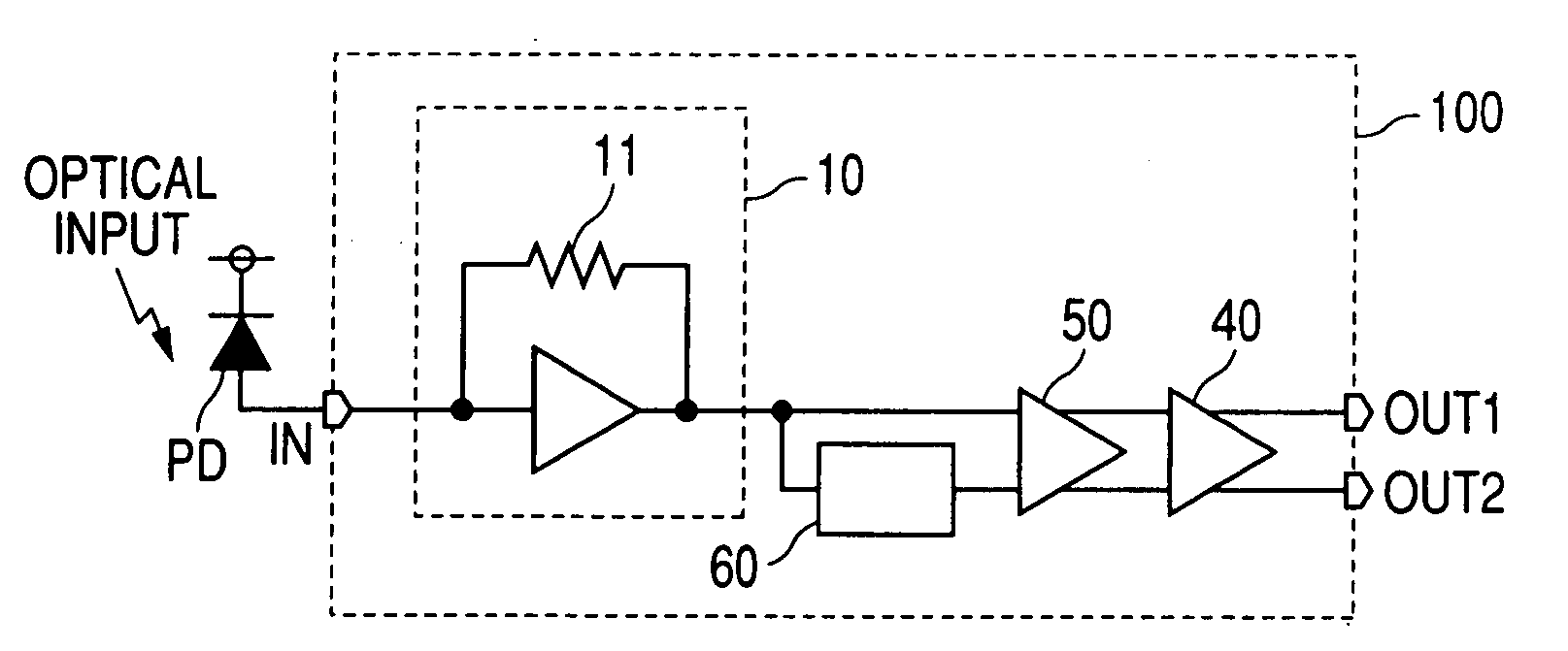
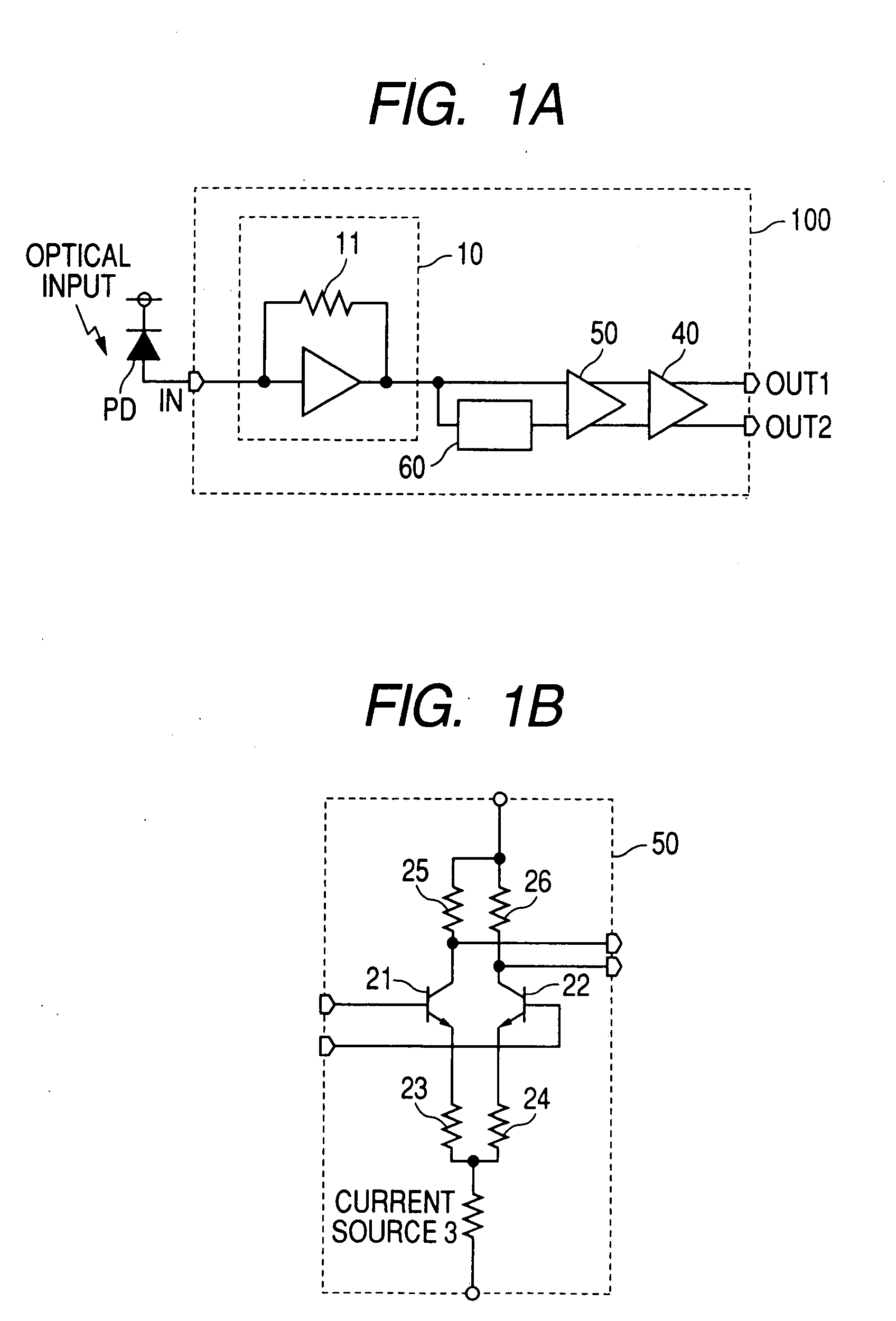
[0038]FIG. 1 shows a first embodiment of the optical signal receiving circuit to which the invention is applied. The optical signal receiving circuit 100 of the present embodiment includes a current-voltage converting circuit 10 receiving the current signal output from a photoelectric converting circuit PD, photodiode, receiving an optical signal and converting the signal into the current signal, as an input signal thereto and converting the current signal into a voltage signal, a voltage generating circuit 60 receiving the voltage signal output from the current-voltage converting circuit 10 as an input thereto and generating a DC voltage from the voltage signal, and a first differential circuit 50 receiving a first voltage signal output from the current-voltage converting circuit 10 and a second voltage signal output from the voltage generating circuit 60 as inputs thereto and generating a differential voltage signal from the first and second voltage signals. The first differential...

second embodiment

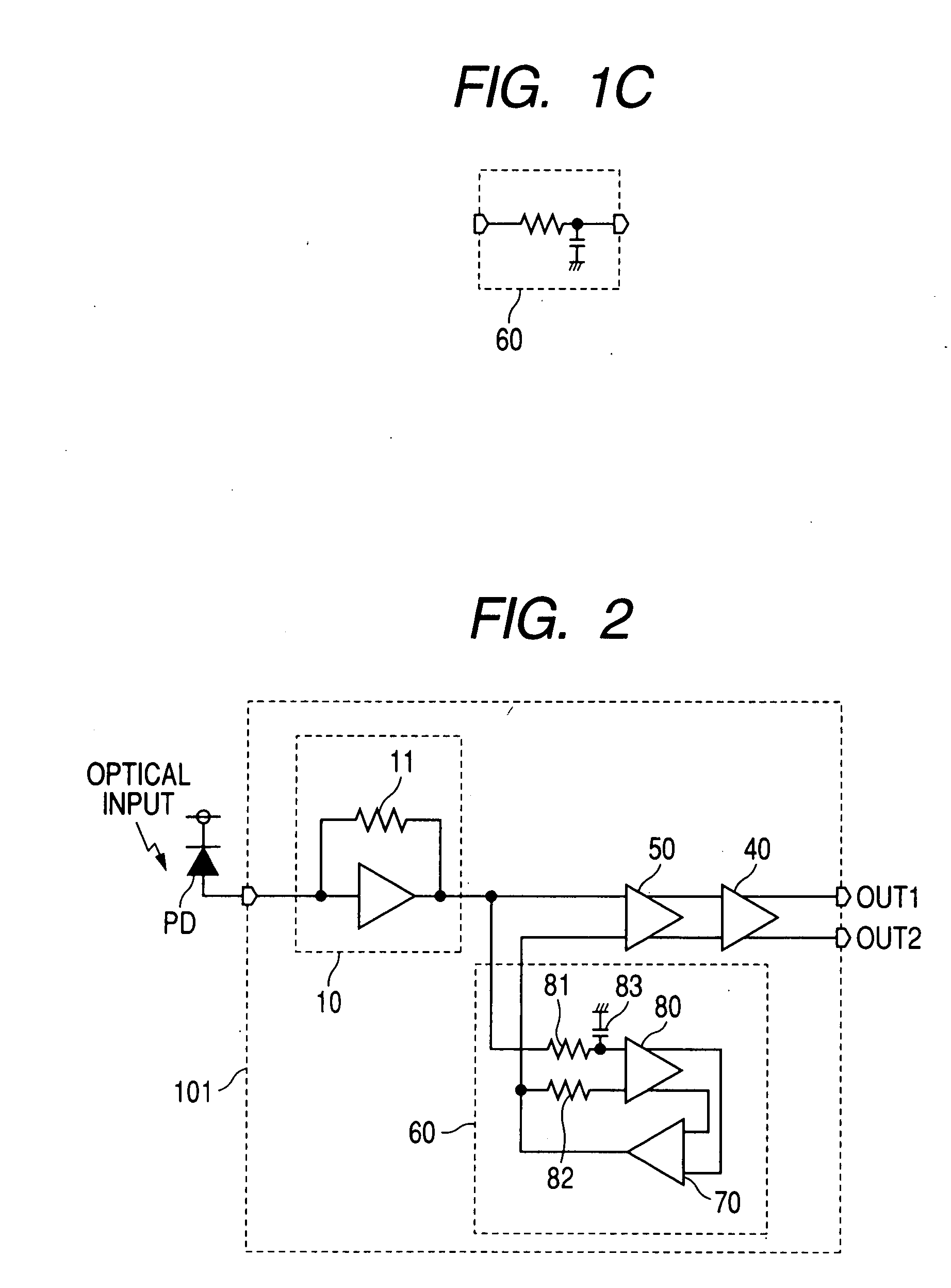
[0055]FIG. 2 shows a second embodiment of the optical signal receiving circuit to which the invention is applied. It differs from the first embodiment in that the voltage generating circuit 60 is configured of a feedback loop using an error amplifier. The voltage generating circuit 60 includes a resistor 81 and a capacitor 83 constituting a low-pass filter, a differential circuit 80, an input-voltage-offset compensating resistor 82 of the differential circuit 80, and an error amplifier 70.

[0056]The voltage signal input to the voltage generating circuit 60 is turned into an average voltage level by extraction of its DC component through the low-pass filter configured of the resistor 81 and the capacitor 83, and the signal is input to one input terminal of the differential circuit 80. At this time, since the amplitude is limited by the low-pass filter and, in addition, the feedback loop does not need wide bandwidth, the differential circuit 80 does not need to use a resistor for its c...


PUM


Abstract

An optical signal receiving circuit has a current-voltage converting circuit which receives the output current signal of a photoelectric converting circuit, converting an optical signal into the current signal, and converts the current signal into a voltage signal. A differential circuit in the subsequent stage to the current-voltage converting circuit uses a resistor as its current source to facilitate setting of an operating voltage level in the circuit. To eliminate an adverse effect of asymmetry of the output waveform from the differential circuit due to the use of the resistor, the reference voltage level as the other input to the reference circuit is generated from the output voltage signal of the current-voltage converting circuit by a voltage generating circuit incorporating a feed-forward-controlling connection. Thus, coexistence of high bandwidth characteristics and broad dynamic range having so far been difficult to attain by low voltage apparatus can be realized.

Description

CLAIM OF PRIORITY[0001]The present application claims priority from Japanese application JP 2006-061996 filed on Mar. 8, 2006, the content of which is hereby incorporated by reference into this application.FIELD OF THE INVENTION[0002]The present invention relates to an optical signal receiving circuit for converting an optical signal into differential voltage signals and, more particularly, relates to an optical signal receiving circuit operable with a single low-voltage power supply of 3.3 V or the like.BACKGROUND OF THE INVENTION[0003]With recent development of widespread use of optical communications, demands are becoming strong for higher-speed transmitting and receiving circuits. Also, small low-voltage and low-power-consumption circuits are highly demanded from the point of view of cost reduction and energy saving.[0004]In optical signal receiving circuits and optical signal receiving apparatuses, such an amplifier is generally needed that performs photoelectric conversion of ...

Claims


Application Information

Patent Timeline
Patent Type & Authority Applications(United States)
IPC IPC(8): H04B10/06H03F3/08H04B10/2507H04B10/40H04B10/50H04B10/60
CPCH04B10/66
Inventor TAKAHASHI, HIDEYUKIYOSHIOKA, HIROYUKIYOSHIDA, HIDEFUMIIRIKURA, SHOGO
Owner HITACHI LTD
Why Eureka
Try Eureka