Semiconductor laser device and optical pickup device

a laser device and semiconductor technology, applied in the direction of optical beam sources, polarising elements, instruments, etc., can solve the problems of affecting the oscillation state of the original laser beam, affecting the power affecting the accuracy of the laser beam, so as to reduce the return light to the semiconductor laser device and low cost

Inactive Publication Date: 2006-09-12
SHARP KK
View PDF26 Cites 9 Cited by
  • Summary
  • Abstract
  • Description
  • Claims
  • Application Information

AI Technical Summary

Benefits of technology

[0020]An object of this invention is to provide a semiconductor laser device and an optical pickup device capable of reducing the return light to the semiconductor laser device at low cost.

Problems solved by technology

Also, these optical pickup devices has a drawback that the return light to the semiconductor laser generates the SCOOP (Self Couple Optical Pickup) phenomena exerting a harmful influence on the oscillation state of the original laser beam.
This causes the reflected return beams to be disadvantageously interfered with the original beam L as optical noises, which leads to significant deterioration of signal detection characteristic and the servo characteristic of the optical pickup device.
In addition, since the reflected main beam Lm fluctuates according to the surface state of the optical disk 6, the power of the laser beam L also disadvantageously fluctuates in accordance with the above-mentioned fluctuation.
However, all of the above-stated methods have difficulties in formation of the reflectors and so on, which causes low productivity of the semiconductor laser devices.
However, the slant surface forming portion, which is provided at the portion 702 to which the maximum pressure is applied as described above, is disadvantageously easily collapsed by pressure.
Therefore, in the case where the slant surface 212 is provided on the portion 111a, extremely poor productivity results.
Accordingly, there is a problem that it is realistically impossible to carry out mass production of the stem 210 that has the header section 211 on which the aforementioned slant surface 212 is directly formed.
However, it is extremely difficult to attach the reflector 113 so as not to bring the reflector 113 in contact with the laser chip 108.
Moreover, when the reflector 113 protrudes from the end of the header section 111, the laser beam L of the laser chip 108 is partially blocked off by the reflector 113 as shown in FIG. 10, and this leads to a problem that the light emission characteristic of the laser chip 108 is degraded.
However, the increase in the reflectance of the light-emitting end surface 108a disadvantageously leads to reduction of a differential efficiency ηd of the laser beam L of the laser chip 108, which reduction is unsuitable for increase of output power or reduction of current in the laser chip 108.
Then, the zero-order diffracted light exerts such a harmful influence on the semiconductor laser 157 as to provide the laser beam with unstable oscillation.

Method used


Image

  • Semiconductor laser device and optical pickup device
  • Semiconductor laser device and optical pickup device
  • Semiconductor laser device and optical pickup device

Examples


first embodiment

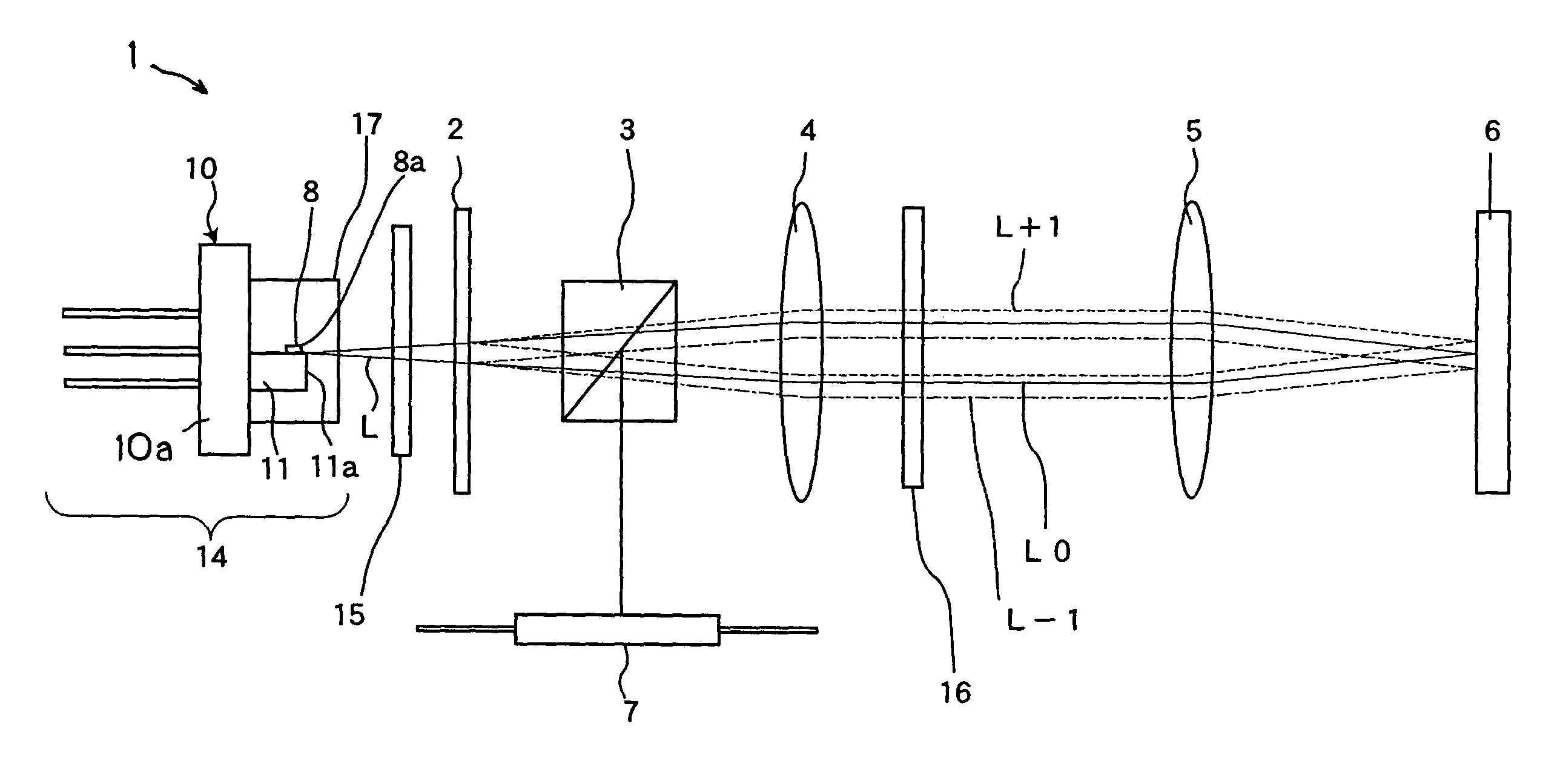
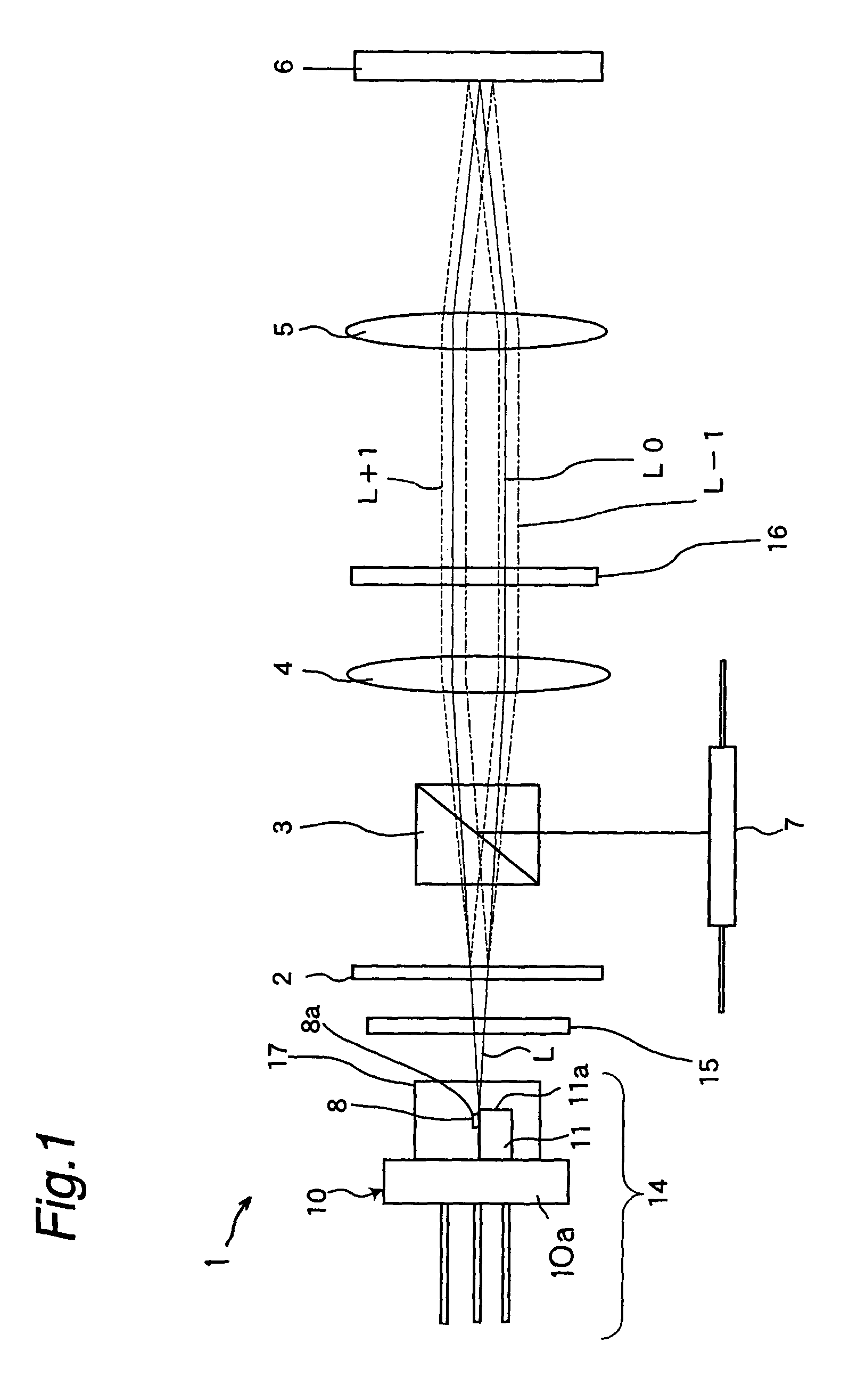
[0088]FIG. 1 shows a schematic construction of a optical pickup device according to a first embodiment of this invention. This optical pickup device includes a semiconductor laser device 1, a 3-beam generating diffraction grating 2, a beam splitter 3, a collimator lens 4, an object lens 5 and a photodetector 7.

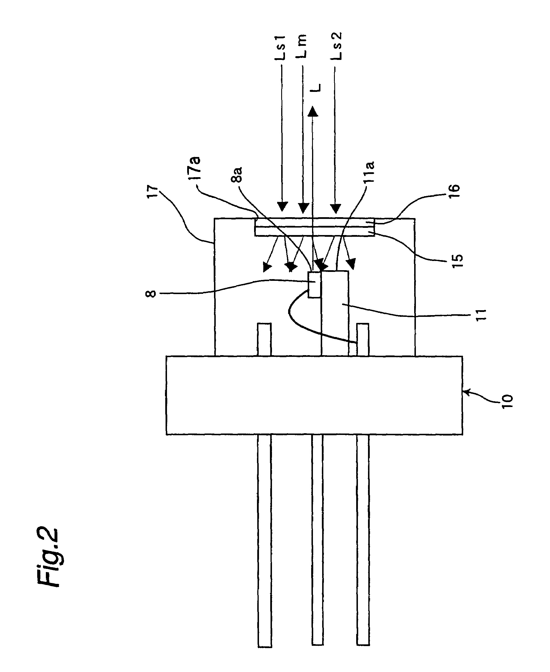
[0089]The semiconductor laser device 1 is constructed of a main body 14 and a polarizing diffraction grating 15. The 3-beam generating diffraction grating 2 is arranged so that light emitted from the main body 14 of the semiconductor laser device 1 passes through the 3-beam generating diffraction grating 2. The collimator lens 4 changes the light which passes through this 3-beam generating diffraction grating 2 into parallel light. The object lens 5 concentrates the parallel light on the surface of an optical disk 6 as an object to be irradiated, that is, an optical recording medium. Between the 3-beam generating diffraction grating 2 and the collimator lens 4, the beam splitt...

second embodiment

[0112]FIG. 3 shows a perspective view of a semiconductor laser device according to a second embodiment of the present invention. FIG. 4 shows a schematic sectional view of an optical pickup device provided with the semiconductor laser device shown in FIG. 3.

[0113]The semiconductor laser device 60 shown in FIG. 3 has a semiconductor laser 37, a hologram device 34 and a light-receiving device 38. The semiconductor laser 37 is a light source for emitting light toward an optical disk 65 as an optical recording medium shown in FIG. 4. The hologram device 34 has a signal hologram 35 and a polarizing diffraction grating 36.

[0114]The signal hologram 35 guides the light reflected on the optical disk 65 toward the light-receiving device 38 for signal detection. The light-receiving device 38 receives light 39 guided by the signal hologram 35. The polarizing diffraction grating 36 diffracts the zero-order diffracted light that is diffracted by the signal hologram 35.

[0115]The semiconductor lase...

third embodiment

[0143]A semiconductor laser device according to a third embodiment of this invention is shown in FIG. 13.

[0144]The semiconductor laser device 80 of the third embodiment has a stem 81 as a base and a semiconductor laser 83 as a light source. The semiconductor laser 83 is mounted on a header section 82 that is a part of the stem 81. The stem 81 is constructed of a base portion 81a and the header section 82 that protrudes from this base portion 81a. A cap 84 which covers the semiconductor laser 83 and the header section 82 is attached to the base portion 81a of the stem 81. The semiconductor laser 83 emits a laser beam L from a light-emitting end surface 83a that is a front end surface of the semiconductor laser 83. The laser beam L is constituted of laser light that includes P-polarized light and S-polarized light.

[0145]A hologram device 85 is attached to a top plate 84a of the cap 84 so as to cover a window (not shown) formed in the top plate 84a. The hologram device 85 includes a po...


PUM

PropertyMeasurementUnit
angleaaaaaaaaaa
angleaaaaaaaaaa
wavelengthaaaaaaaaaa

Abstract

A semiconductor laser device has a semiconductor laser and a polarizing diffraction grating that is arranged ahead of the semiconductor laser. A reflected light from an optical recording medium is diffracted by the polarizing diffraction grating according to the polarization direction of the reflected light. The reflected light is thereby deviated from the direction toward the semiconductor laser to prevent the reflected light from returning to the semiconductor laser.

Description

BACKGROUND OF THE INVENTION[0001]This invention relates to a semiconductor laser device and an optical pickup device, and in particular to an optical pickup device for use in an apparatus for optically recording or reproducing information on an information recording medium. This invention also relates to a semiconductor laser device and an optical pickup device that have a hologram device, and in particular to a semiconductor laser device and an optical pickup device for use in reading and writing a signal on an optical recording medium.[0002]Conventionally there has been an optical pickup device as shown in FIG. 5. A laser chip 108 in a semiconductor laser device 101 of the optical pickup device emits a laser beam L which is incident on a diffraction grating 102. The laser beam L is split into a main beam L0 and two side beams L+1 and L−1 by the diffraction grating 102. The three beams (main beam L0 and side beams L+1 and L−1) are transmitted through a beam splitter 103 and transmi...

Claims


Application Information

Patent Timeline
Patent Type & Authority Patents(United States)
IPC IPC(8): H01S5/00G02B5/18G02B5/30G02B5/32G11B7/00G11B7/12G11B7/123G11B7/125G11B7/135G11B7/1353H01S3/04H01S5/022
CPCG11B7/1353G11B7/1205G11B7/123G11B7/127
Inventor SHINOHARA, HISAYUKIARIYOSHI, AKIRAHAMAOKA, OSAMU
Owner SHARP KK
Why Eureka
Try Eureka