Interference signal decoupling on a printed circuit board

a technology of interference signal and printed circuit board, which is applied in the direction of electrical apparatus construction details, line-transmission details, non-metallic protective coating applications, etc., can solve the problems of limiting the shielding effectiveness of components, reducing the shielding effect, and increasing the difficulty of maintaining sufficient electrical noise isolation and limiting inductance between components

Inactive Publication Date: 2006-09-19
HEWLETT PACKARD DEV CO LP
View PDF4 Cites 54 Cited by
  • Summary
  • Abstract
  • Description
  • Claims
  • Application Information

AI Technical Summary

Problems solved by technology

As switching rates increase, problems which do not exist at lower speeds, such as shielding electronics from external sources of electromagnetic interference (EMI), become increasingly problematic.
Moreover, maintaining sufficient electrical noise isolation and limiting inductance between components becomes more difficult as the frequency at which a circuit operates increases.
Such metallic enclosures have numerous drawbacks that limit their shielding effectiveness.

Method used


Image

  • Interference signal decoupling on a printed circuit board
  • Interference signal decoupling on a printed circuit board
  • Interference signal decoupling on a printed circuit board

Examples


example 1

Boron Nitride & Acrylic Dispersion 1500

[0089]

Thermal loading material 1400:10%–80% BN, 0.1–10 micron powderBinder 1504:90%–20% AcrylicBase Liquid 1506:water or organic solventCuring:UV or thermally cured

The binder 1504 and base liquid 1506 can be provided in the above-noted acrylic intermediate dispersions. In accordance with the present invention, such intermediate dispersions are doped with the specified thermal loading material 1400 to form one embodiment of thermally conductive dielectric dispersion 1500.

example 2

Boron Nitride & Urethane Dispersion 1500

[0090]

Thermal loading material 1400:10%–80% BN, 0.1–10 micron powderBinder 1504:90%–20% UrethaneBase Liquid 1506:water or organic solventCuring:UV and / or thermally cured

The binder 1504 and base liquid 1506 can be provided in the above-noted urethane intermediate dispersions. In accordance with the present invention, such intermediate dispersions are doped with the specified thermal loading material 1400 to form one embodiment of thermally conductive dielectric dispersion 1500.

example 3

Aluminum Oxide & Acrylic Dispersion 1500

[0091]

Thermal loading material 1400:10%–80% Al2O3, 100 mesh, 99%corundum, alpha-phaseBinder 1504:90%–20% AcrylicBase Liquid 1506:water or organic solventCuring:UV or thermally cured

The binder 1504 and base liquid 1506 can be provided in the above-noted acrylic intermediate dispersions: In accordance with the present invention, such intermediate dispersions are doped with the specified thermal loading material 1400 to form one embodiment of thermally conductive dielectric dispersion 1500.


PUM


Abstract

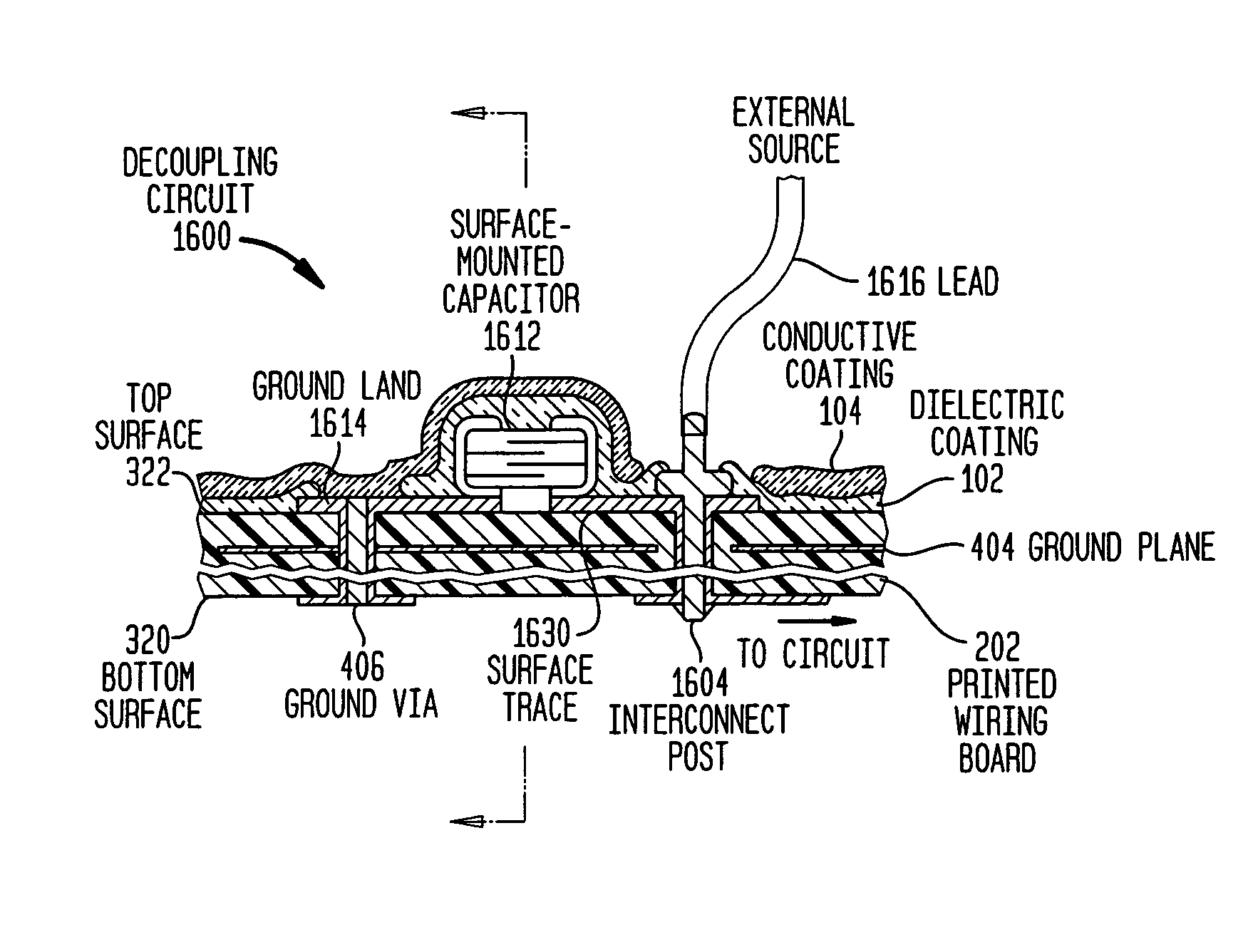
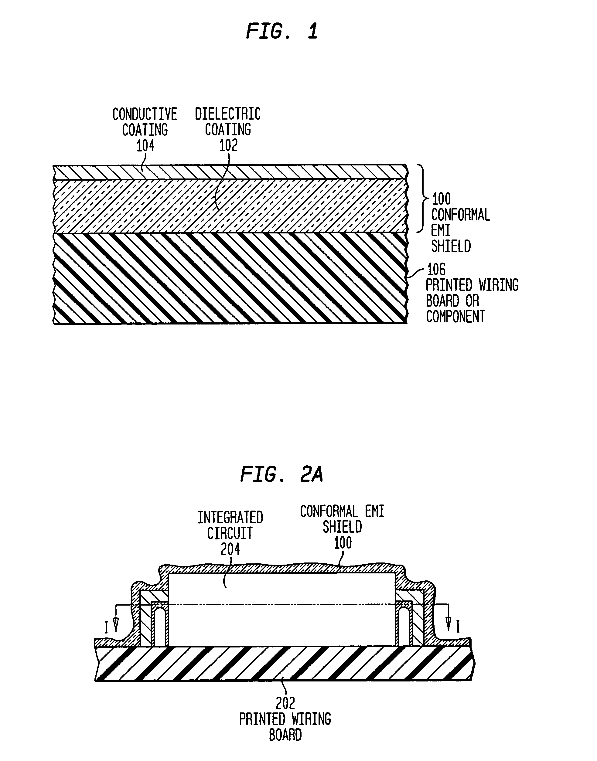
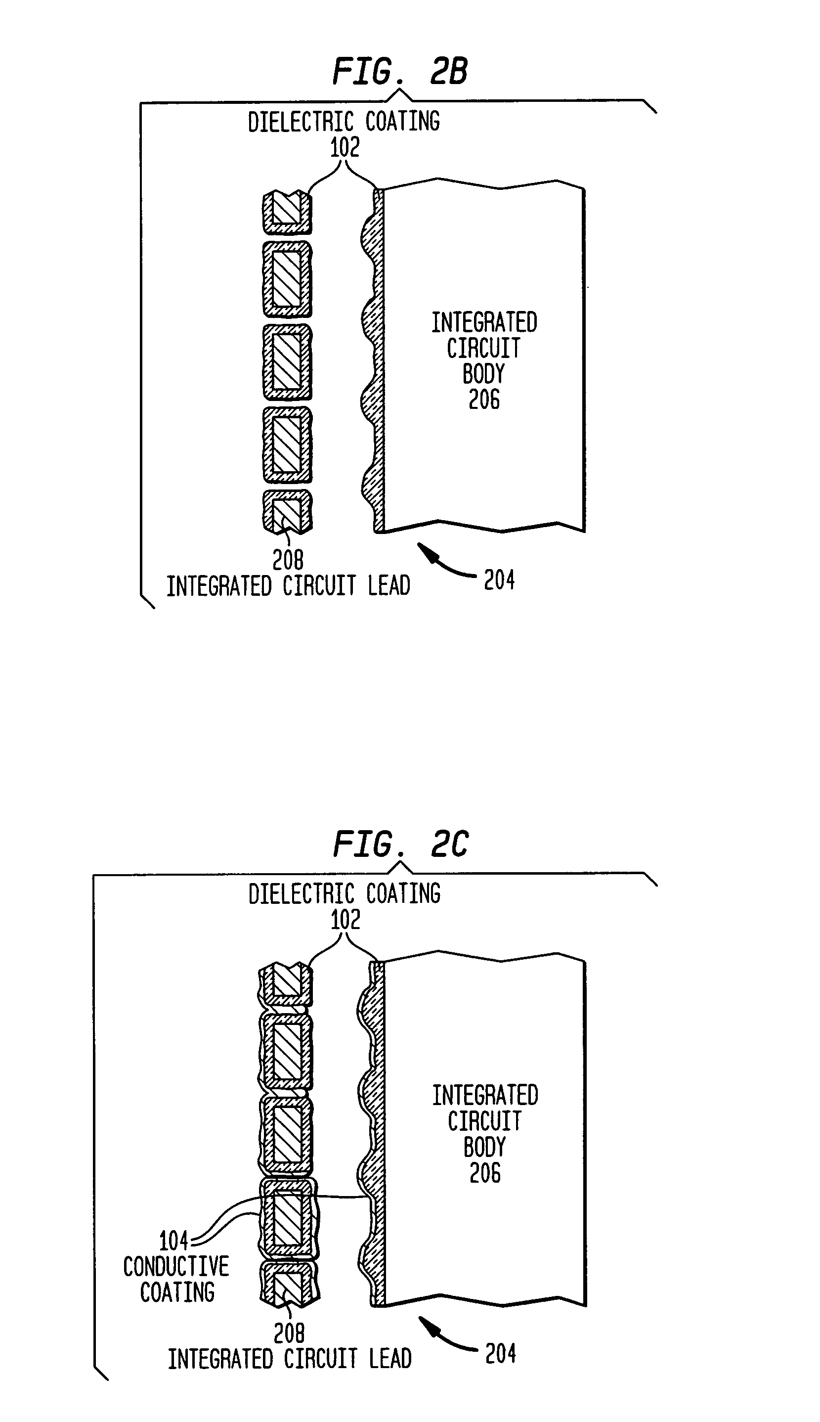
A decoupling circuit on a printed circuit board is disclosed. The decoupling circuit comprises an electrical filter circuit electrically connected between an interconnect post and a ground land of the printed circuit board. The ground land is connected to a ground plane in the printed circuit board. The electrical filter shunts conducted interfering signals received at the interconnect post to the ground plane. Components of the electrical filter circuit and ground plane form a first receiver loop in which induced interfering signals can be generated. The decoupling circuit also comprises a second receiver loop comprising a conductive coating of an EMI shield conformingly adhered to surfaces of the decoupling circuit, and a conductive path of the first receiver loop. The second receiver loop is adapted to have induced therein a signal having a direction and magnitude sufficient to cancel interfering signals induced in the first receiver loop.

Description

CROSS REFERENCE TO RELATED APPLICATION(S)[0001]This is a continuation of application Ser. No. 10 / 079,638, filed Feb. 19, 2002, now U.S. Pat. No. 6,717,485.RELATED APPLICATIONS[0002]The present application is related to the following commonly-owned U.S. patent applications:[0003]U.S. patent application Ser. No. 09 / 812,274 entitled “A BOARD-LEVEL EMI SHIELD THAT ADHERES TO AND CONFORMS WITH PRINTED CIRCUIT BOARD COMPONENT AND BOARD SURFACES,” naming as inventors Samuel M. Babb, Lowell E. Kolb, Brian Davis, Jonathan P. Mankin, Kristina L. Mann, Paul H. Mazurkiewicz and Marvin Wahlen;[0004]U.S. patent application Ser. No. 09 / 813,257 entitled “FILLER MATERIAL AND PRETREATMENT OF PRINTED CIRCUIT BOARD COMPONENTS TO FACILITATE APPLICATION OF A CONFORMAL EMI SHIELD,” naming as inventor Lowell E. Kolb;[0005]U.S. patent application Ser. No. 09 / 812,662 entitled “A LOW PROFILE NON-ELECTRICALLY-CONDUCTIVE COMPONENT COVER FOR ENCASING CIRCUIT BOARD COMPONENTS TO PREVENT DIRECT CONTACT OF A CONFOR...

Claims


Application Information

Patent Timeline
Patent Type & Authority Patents(United States)
IPC IPC(8): H04B3/28H05K1/00H05K9/00H04B15/02H05K1/02H05K3/28
CPCH04B15/02H05K9/0024H05K1/0218H05K3/284
Inventor KOLB, LOWELL E.BABB, SAMUEL M.
Owner HEWLETT PACKARD DEV CO LP
Why Eureka
Try Eureka