Circuit device with a contact element for electrically connecting a wave guide and a conductor strip in a nearly stress-free manner

Inactive Publication Date: 2006-09-19
ROBERT BOSCH GMBH
3 Cites 5 Cited by

AI-Extracted Technical Summary

Problems solved by technology

This fabrication method is very expensive.
Furthermore the electrical connection is put under great mechanical stress by possib...

Benefits of technology

[0013]Thus simple but precise or exact fabrication methods are possible for the leaf spring. Tolerances of <±10 μm may be obtained for the above-described contact element with UV depth lithography. A wide range of materials can be selected so that special...

Abstract

The circuit device has a contact element, which electrically connects a wave guide (1) with a conductor strip (2). To avoid mechanical stresses due to thermal expansion the contact element is a pre-stressed prefabricated leaf spring having reproducible properties, which is bonded at one contacting area to the wave guide (1) or the conductor strip (2) by electrically conducting adhesive or glue, while a sliding contact is provided on the conductor strip (2) or the wave guide (1) at the other contacting area. The prefabricated leaf spring is preferably a MIGA leaf spring precisely made by UV depth lithography and multiplayer galvanic methods in a batch production process.

Application Domain

Multiple-port networksContact member manufacturing +4

Technology Topic

Batch productionPre stressing +13

Image

  • Circuit device with a contact element for electrically connecting a wave guide and a conductor strip in a nearly stress-free manner
  • Circuit device with a contact element for electrically connecting a wave guide and a conductor strip in a nearly stress-free manner
  • Circuit device with a contact element for electrically connecting a wave guide and a conductor strip in a nearly stress-free manner

Examples

  • Experimental program(2)

Example

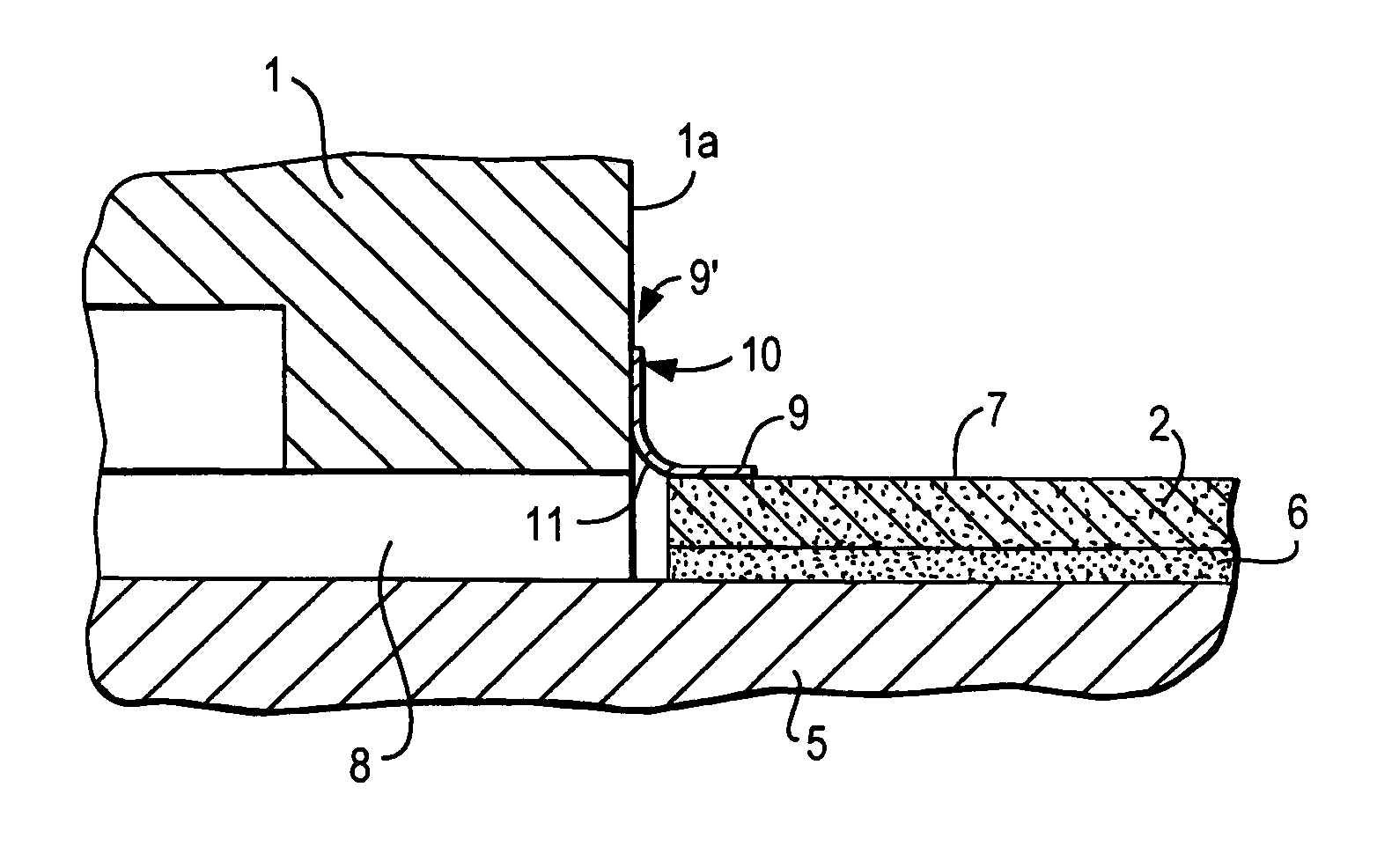
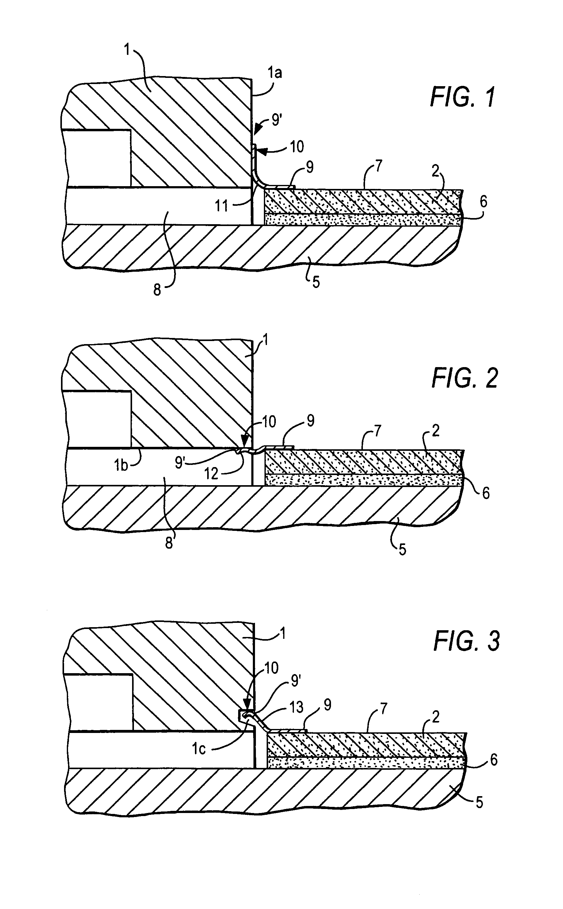
[0024]This latter situation in regard to FIG. 2 is also true of the third embodiment shown in FIG. 3. In the embodiment shown in FIG. 3, the leaf spring 13 is bonded to the conductor strip 7 at a first contacting area 9 with an electrically conductive glue or adhesive. The sliding contact 10 of the leaf spring 13 with the wave guide 1 is located at another contacting area 9′ in a cavity 1c of the wave guide 1. It is also possible to additionally secure the spring contact in the cavity with a highly flexible electrically conductive glue or adhesive material.
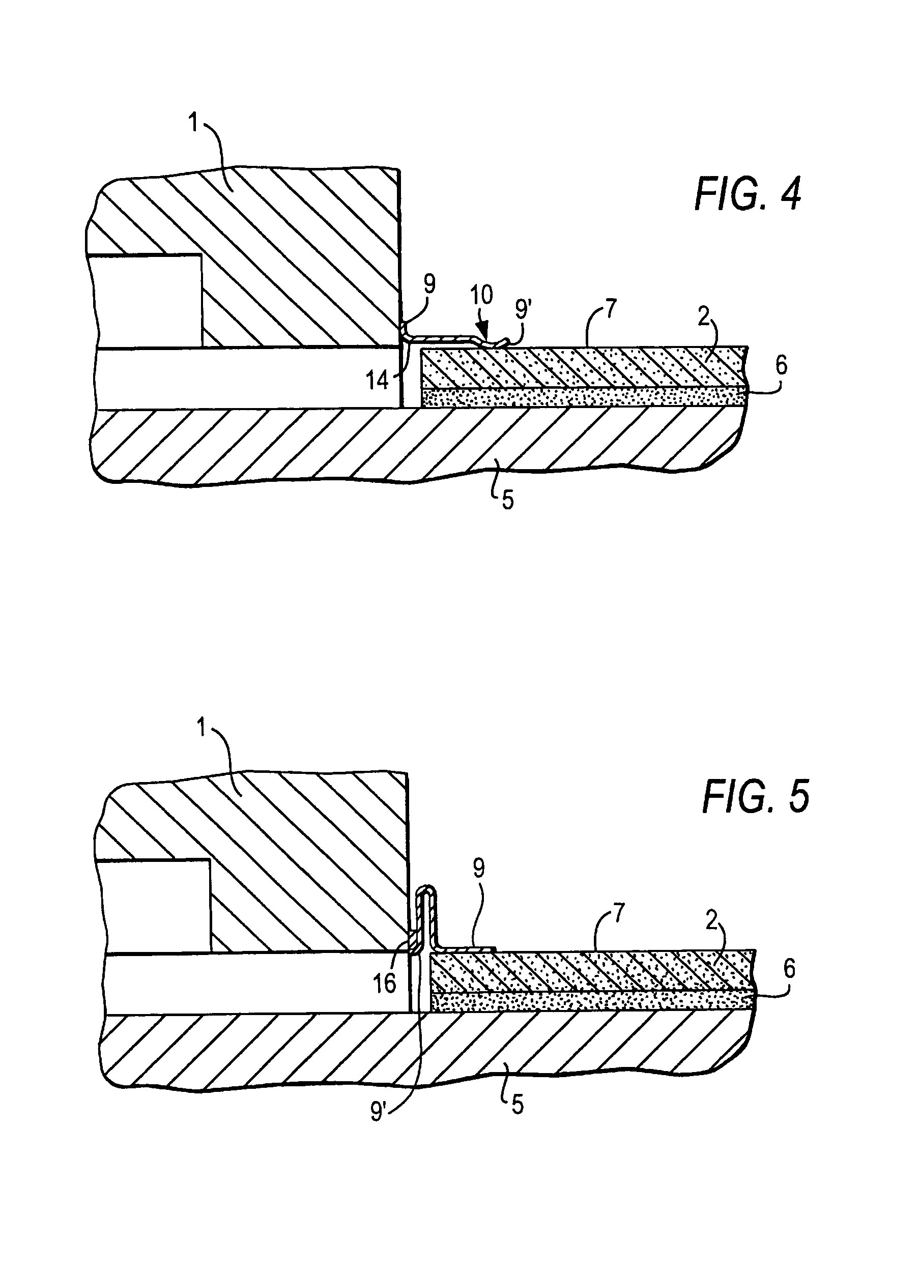
[0025]In the embodiment shown in FIG. 4, a leaf spring 14 is electrically conductively glued to the wave guide 1 at one contacting area 9, while the sliding contact 10 makes electrical contact on the conductor strip 7 on the other conducting area 9′.

Example

[0026]In FIG. 5, in a fifth embodiment, the leaf spring 15 has a curved U-shape. A first contacting area 9 of the leaf coil spring 15 is glued in an electrically conductive manner to the conductor strip 7. The other contacting area 9′ of the leaf spring 15 is formed as an electrically conducting adhesive area 16. This adhesive area 16 can however be highly flexible. The leaf spring 15 need not then be formed so that it is U-shaped.
[0027]The disclosure in German Patent Application 199 02 240.2 of Jan. 21, 1999 is incorporated here by reference. This German Patent Application describes the invention described hereinabove and claimed in the claims appended hereinbelow and provides the basis for a claim of priority for the instant invention under 35 U.S.C. 119.
[0028]While the invention has been illustrated and described as embodied in a circuit device with a contact element for electrically connecting a wave guide and a conductor strip in a nearly stress-free manner, it is not intended to be limited to the details shown, since various modifications and changes may be made without departing in any way from the spirit of the present invention.
[0029]Without further analysis, the foregoing will so fully reveal the gist of the present invention that others can, by applying current knowledge, readily adapt it for various applications without omitting features that, from the standpoint of prior art, fairly constitute essential characteristics of the generic or specific aspects of this invention.

PUM

PropertyMeasurementUnit
Length1.0E-5m
Thickness5.0E-5m
Thickness1.0E-4 ~ 2.0E-4m

Description & Claims & Application Information

We can also present the details of the Description, Claims and Application information to help users get a comprehensive understanding of the technical details of the patent, such as background art, summary of invention, brief description of drawings, description of embodiments, and other original content. On the other hand, users can also determine the specific scope of protection of the technology through the list of claims; as well as understand the changes in the life cycle of the technology with the presentation of the patent timeline. Login to view more.

Similar technology patents

Electronic component mounted structure and method of manufacturing the same

InactiveUS20090246474A1good connection reliabilityeasily manufacture
Owner:PANASONIC CORP

Classification and recommendation of technical efficacy words

  • easily manufacture

Dispensing system

ActiveUS20070278164A1easily manufactureprevent theft
Owner:WESTROCK SHARED SERVICES LLC

Reciprocating compressor and manufacturing method thereof

InactiveUS20060024181A1easily manufactureprevent abrasion
Owner:LG ELECTRONICS INC
Why Eureka
Try Eureka