Wideband antenna array

a wideband antenna and array technology, applied in the direction of slot antennas, antennas, basic electric elements, etc., can solve the problems of inherently narrowband arrays of patch antennas, inability to make small elements small enough to avoid grating lobes, and low-cost fabrication methods

Inactive Publication Date: 2006-09-19
HRL LAB
View PDF18 Cites 174 Cited by
  • Summary
  • Abstract
  • Description
  • Claims
  • Application Information

AI Technical Summary

Problems solved by technology

Although PCB technology provides a potentially low-cost fabrication method, prior art arrays of patch antennas are inherently narrowband due to the narrowband nature of the radiating elements, i.e., the patches.
Although these elements are inherently wideband, they require a large area (relative to a wavelength of the frequencies of interest) and the element spacing cannot be made small enough to avoid grating lobes for scans at low elevation angles.
Thus, these prior art wideband elements severely limit the achievable field of view of the array.
Although this antenna is wideband and can be closely spaced to neighboring elements, the dielectric rod is not inherently compatible with PCB technology.
This antenna suffers the limitations described above, specifically that the bandwidth is very low, a few percent at most.
Although this does increase the array bandwidth somewhat, patches remain inherently narrowband and the overall array bandwidth remains low.
This restriction limits the amount of scanning that can be accomplished (i.e., the antenna field of view) since excessive scanning will result in grating lobes unless the inter-element spacing can be kept near half a free space wavelength.
This modular architecture allows each individual element to be manufactured separately; however, high gain antenna arrays that require thousands of elements are extremely expensive.

Method used


Image

  • Wideband antenna array
  • Wideband antenna array
  • Wideband antenna array

Examples


Embodiment Construction

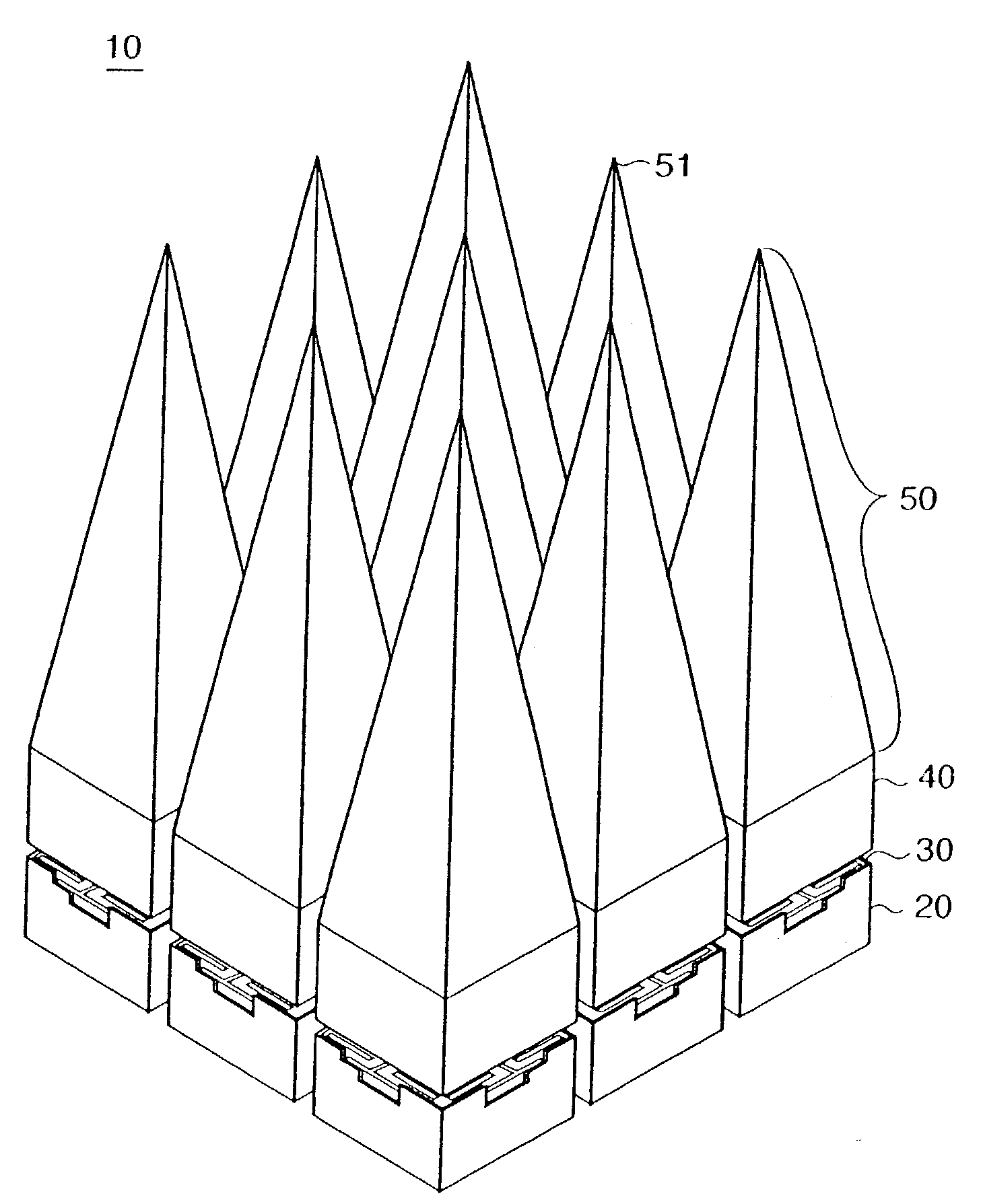
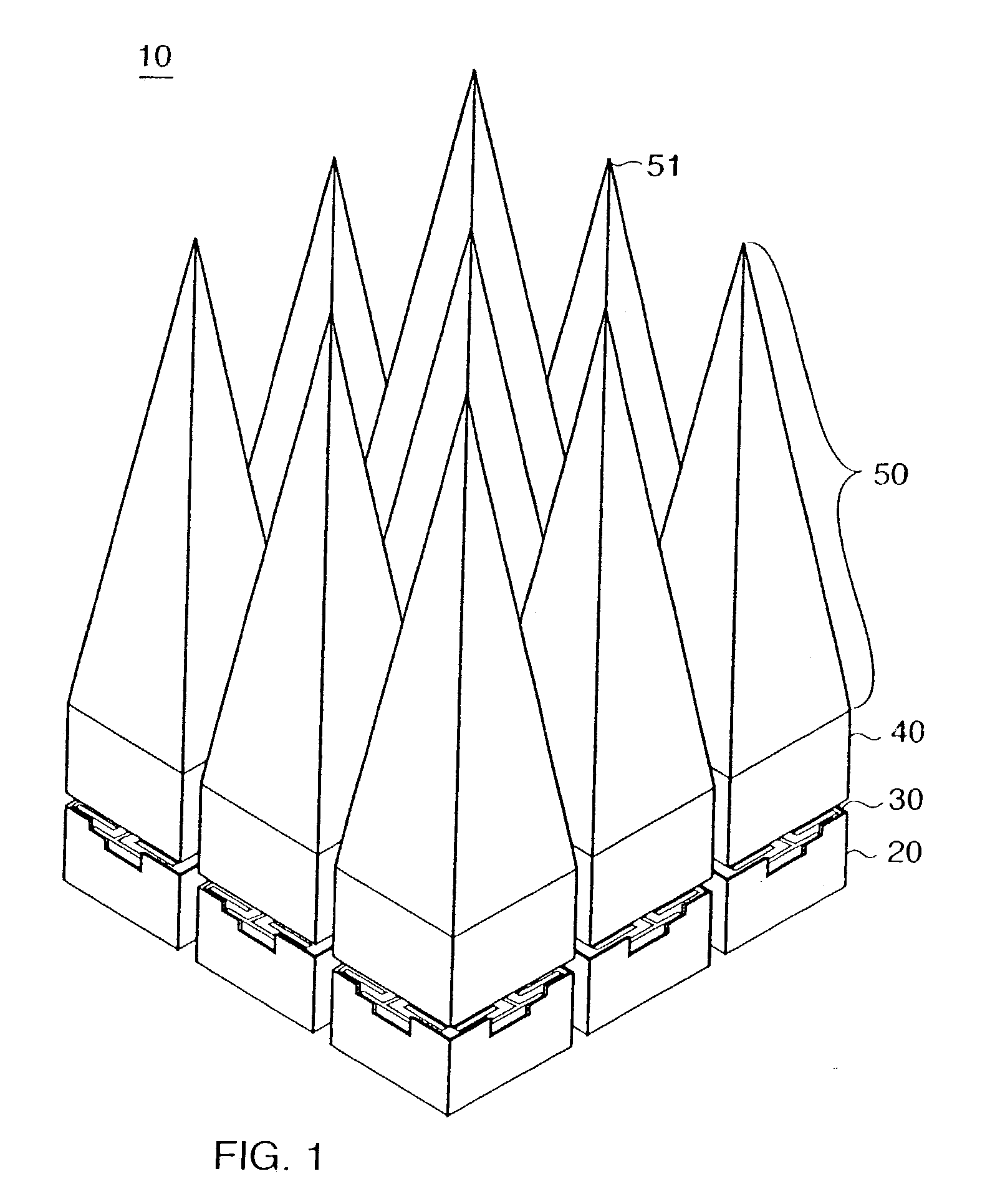
[0025]FIG. 1 is a schematic of a 3×3 array of the co-planar waveguide (CPW) to freespace transition structure 10. The basic array element is a simple CPW fed parallel plate waveguide structure with a gradual, tapered transition to freespace. The structure 10 can be broken down into four different sections: an optional lower parallel plate waveguide section 20; a circuit board layer that contains the CPW probe and active electronics 30; an upper parallel plate waveguide section 40; and a substrate to freespace transition 50. FIGS. 2 through 5 detail each of the three lower sections.

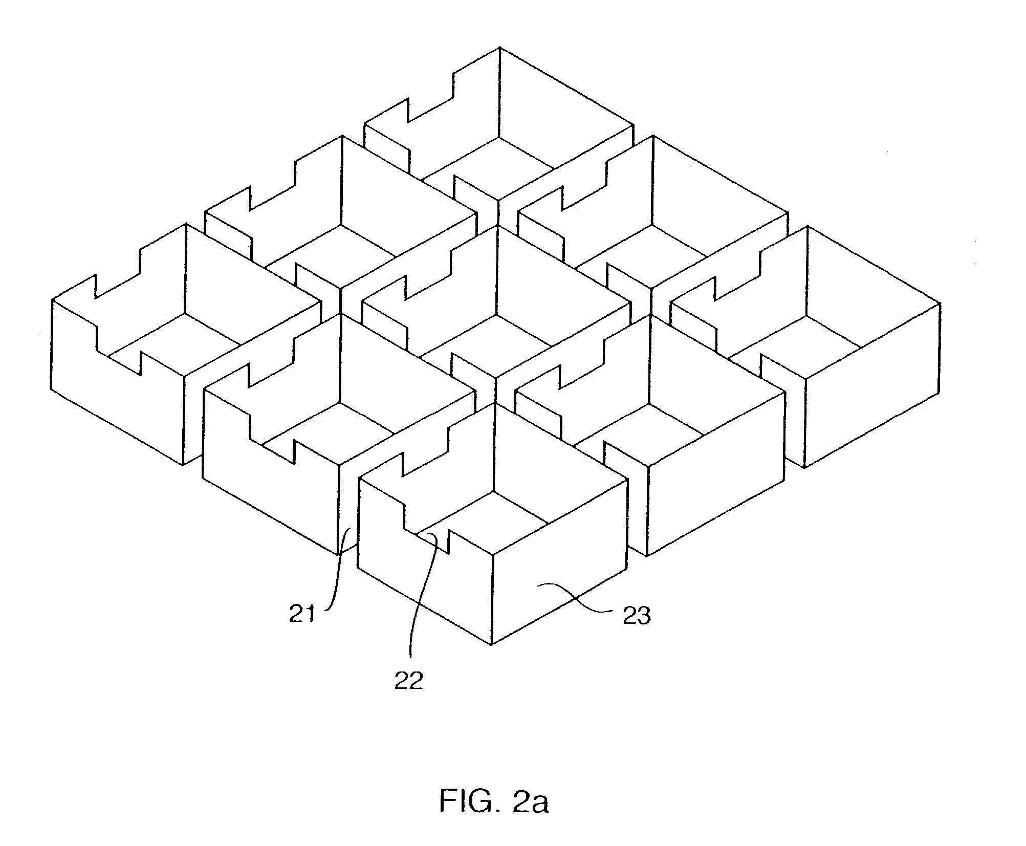
[0026]The optional portion 20 of the structure 10 is shown in FIG. 2a. The optional portion 20 defines a series of crisscrossed parallel plate waveguides 21 formed by walls 23 defining box-shaped structures. The box-shaped structure can take the shape of a square or a rectangle. At the top of one wall for each of these parallel plate waveguides 21 is a rectangular aperture or notch 22 to accommodate a CPW ...


PUM


Abstract

An antenna array comprises a substrate; a plurality of projecting, tapering structures disposed in an array and attached to a first major surface of said substrate, the plurality of projecting, tapering structures defining a plurality of waveguides therebetween; and a plurality of box-shaped structures disposed in an array and attached to a second major surface of the substrate, the plurality of box-shaped structures defining a plurality of waveguides therebetween, the plurality of waveguides defined by the plurality of projecting, tapering structures aligning with the plurality of waveguides defined by the plurality of box-shaped structures. The substrate includes a plurality of probes for feeding the plurality waveguides.

Description

[0001]This application claims benefit of U.S. Ser. No. 60 / 378,151, filed on May 14, 2002.TECHNICAL FIELD[0002]This invention relates to a novel method of achieving wideband electronically scanned antenna performance over a wide field of view with a structure that is very easy to fabricate and integrate with both standard microwave printed circuits and electronics. In particular, it relates to a wide bandwidth co-planar waveguide (CPW) to freespace transition constructed by attaching simple elongated radiating elements directly to printed circuit boards (PCBs).[0003]This invention has both commercial and military applications. On the commercial side, this invention will allow a low cost electronically scanned antenna (ESA) to be available for terrestrial terminals in direct broadcast satellite and commercial marine applications. On the military side, this invention is applicable to battlefield communications via satellite, as well as advanced antenna concepts such as a distributed di...

Claims


Application Information

Patent Timeline
Patent Type & Authority Patents(United States)
IPC IPC(8): H01Q13/10H01Q21/00
CPCH01Q21/0087H01Q21/0006
Inventor LYNCH, JONATHAN J.COLBURN, JOSEPH S.
Owner HRL LAB
Why Eureka
Try Eureka