Thin film transistor array substrate and method for repairing the same

a technology of thin film transistors and array substrates, which is applied in the direction of instruments, semiconductor devices, optics, etc., can solve the problems of increasing power consumption, difficult to manufacture and increasing the difficulty of manufacturing a tft array substrate with substantially no point defects

Active Publication Date: 2006-09-19
SHARP KK
View PDF9 Cites 7 Cited by
  • Summary
  • Abstract
  • Description
  • Claims
  • Application Information

AI Technical Summary

Benefits of technology

[0019]Therefore, it is an object of the present invention to provide a TFT array substrate with an improved auxiliary capacitor structure that can maintain the aperture ratio high while achieving reliability in inspection for point defects.

Problems solved by technology

In reality, millions of TFTs are often formed on a substrate, and it is difficult to manufacture a TFT array substrate with substantially no point defects.
If, in this TFT array substrate, malfunction or bad electrical contact occurs in a TFT, a voltage is not supplied to the pixel electrode 112, which results in a point defect.
This leads to increase of power consumption.
Along with the structural problem, that is, the reduced aperture ratio, of the conventional TFT array substrate, the problems in the conventional repair methods degrade the image quality of a liquid crystal panel.

Method used


Image

  • Thin film transistor array substrate and method for repairing the same
  • Thin film transistor array substrate and method for repairing the same
  • Thin film transistor array substrate and method for repairing the same

Examples


Embodiment Construction

[0044]The preferred embodiments of the invention are now described with reference to the accompanying drawings.

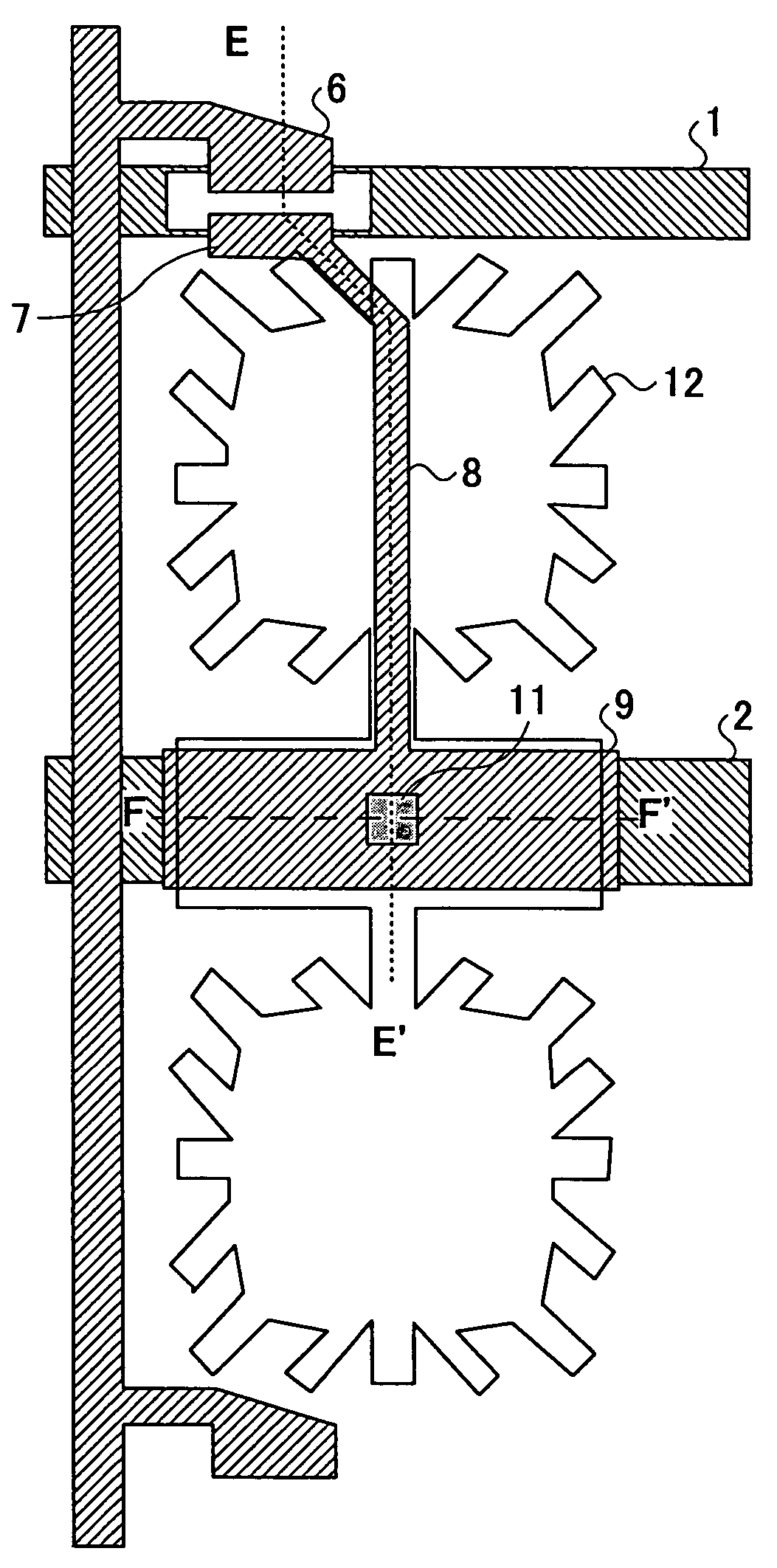
[0045]FIG. 3 and FIG. 4 illustrate a TFT array substrate according to an embodiment of the invention. FIG. 4A is a cross-sectional view taken along the E–E′ line shown in FIG. 3, and FIG. 4B is a cross-sectional view taken along the F–F′ line. The TFT array substrate shown in FIG. 3 and FIG. 4 is conceived and proposed in an attempt to solve the problem of the reduced aperture ratio of the conventional TFT array substrates, in the process of achieving the TFT array substrate shown in FIG. 5 and FIG. 6.

[0046]To maintain the aperture ratio high, the source electrode 7 and the middle electrode (or the opposite electrode) 9 facing the auxiliary capacitor electrode 2 are connected by a connection 8, which is formed in the same layer as the source electrode 7 and the middle electrode 9. The source electrode 7 is connected directly to the middle electrode 9 without relying on the ...


PUM

PropertyMeasurementUnit
areasaaaaaaaaaa
areaaaaaaaaaaa
electricaaaaaaaaaa

Abstract

A thin film transistor array substrate includes an insulating substrate; a thin film transistor arranged in a part of a pixel area on the insulating substrate; an auxiliary capacitor having an auxiliary capacitor electrode arranged in the pixel area and an opposite electrode facing the auxiliary capacitor electrode via an insulating layer, the opposite electrode being located in the same layer as source and drain electrodes of the thin film transistor; and a pixel electrode formed in the pixel area. The opposite electrode is divided into two or more sections, and each of the sections is electrically connected to the pixel electrode via a contact hole.

Description

BACKGROUND OF THE INVENTION[0001]1. Field of the Invention[0002]The present invention generally relates to a thin film transistor (TFT) array substrate and a repair method for a TFT array substrate, and more particularly, to an auxiliary capacitor structure of a TFT array substrate used in display apparatuses and a method for repairing point defect produced during the fabrication process of the TFT array substrate.[0003]2. Description of the Related Art[0004]In recent years and continuing, cost reduction and improved image quality are demanded for display units of information technology equipment. Such demand is especially remarkable for liquid crystal displays (LCDs) used in cellular phones, personal digital assistants, notebook PCs, view finders of video cameras, and the like.[0005]In a liquid crystal display, liquid crystal is sandwiched between a TFT array substrate, in which an array of thin film transistors is formed for driving pixels, and an opposite substrate. Displayed ima...

Claims


Application Information

Patent Timeline
Patent Type & Authority Patents(United States)
IPC IPC(8): G02F1/1343G02F1/1362G02F1/1368H01L27/12
CPCG02F1/134336H01L27/12G02F1/136259
Inventor MATSUI, AKIHIROFUJIKAWA, TETSUYA
Owner SHARP KK
Why Eureka
Try Eureka