Sensing component used to monitor material buildup and material erosion of consumables by optical emission

a technology of optical emission and sensing component, which is applied in the field of plasma processing, can solve the problems of consumable nature of replaceable components that can require frequent maintenance of the plasma processing system, the system is completely broken, and the plasma processing performance is gradually degraded. to achieve the effect of convenient determination

Inactive Publication Date: 2006-09-19
TOKYO ELECTRON LTD
View PDF6 Cites 12 Cited by
  • Summary
  • Abstract
  • Description
  • Claims
  • Application Information

AI Technical Summary

Benefits of technology

[0008]Another object of the invention is to provide a discreet sensing component that can be placed on or near a semiconductor processing part to facilitate accurate determination of when the processing part should be replaced or cleaned.

Problems solved by technology

The erosion or coating of exposed components in the plasma processing system can lead to a gradual degradation of the plasma processing performance and ultimately to complete failure of the system.
The consumable nature of the replaceable components can require frequent maintenance of the plasma processing system.
This frequent maintenance can produce costs associated with plasma processing down-time and new plasma processing chamber components, which can be excessive.
These methods can result in overdue or premature replacement of consumable system components.

Method used


Image

  • Sensing component used to monitor material buildup and material erosion of consumables by optical emission
  • Sensing component used to monitor material buildup and material erosion of consumables by optical emission
  • Sensing component used to monitor material buildup and material erosion of consumables by optical emission

Examples


Embodiment Construction

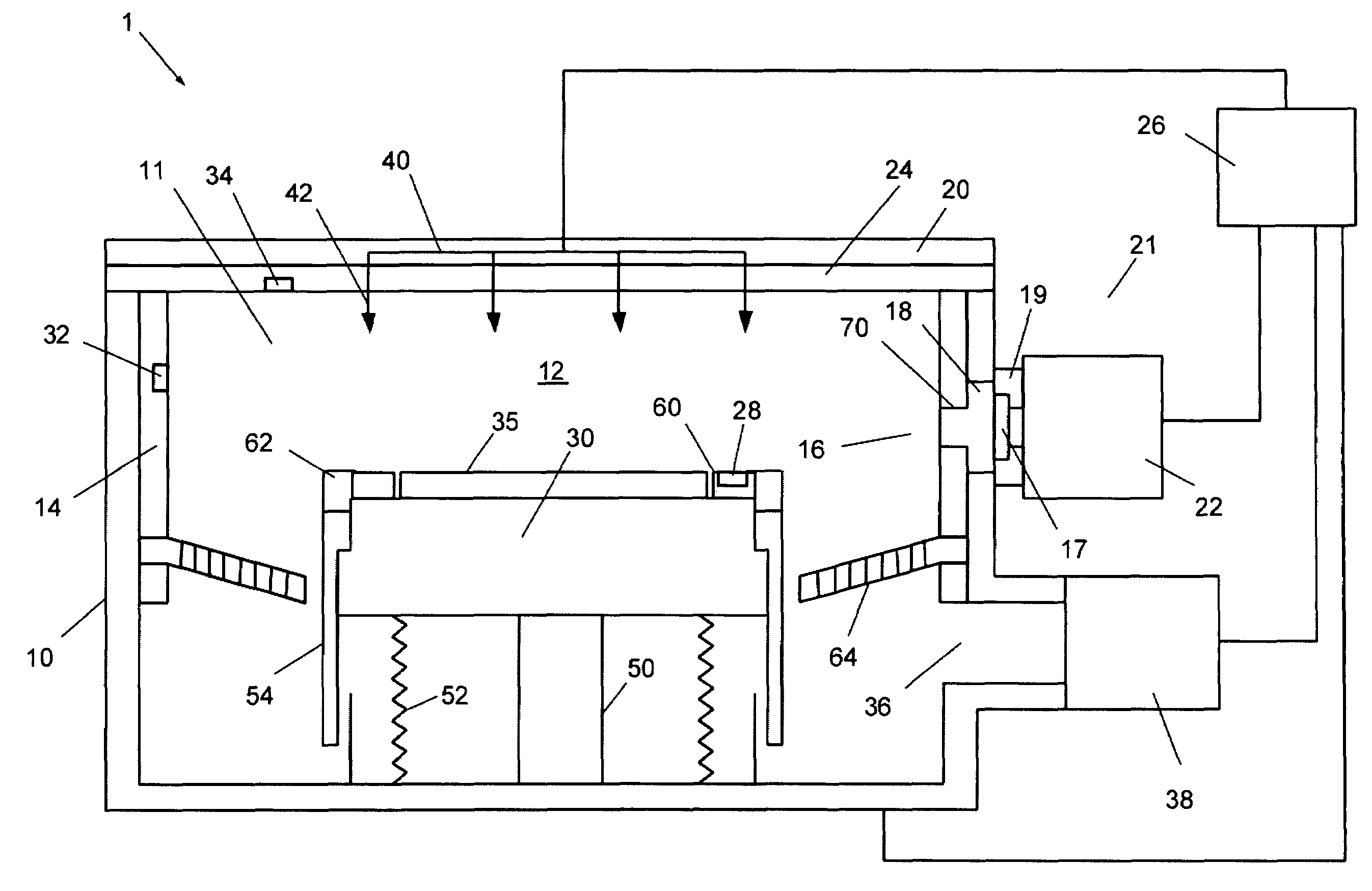
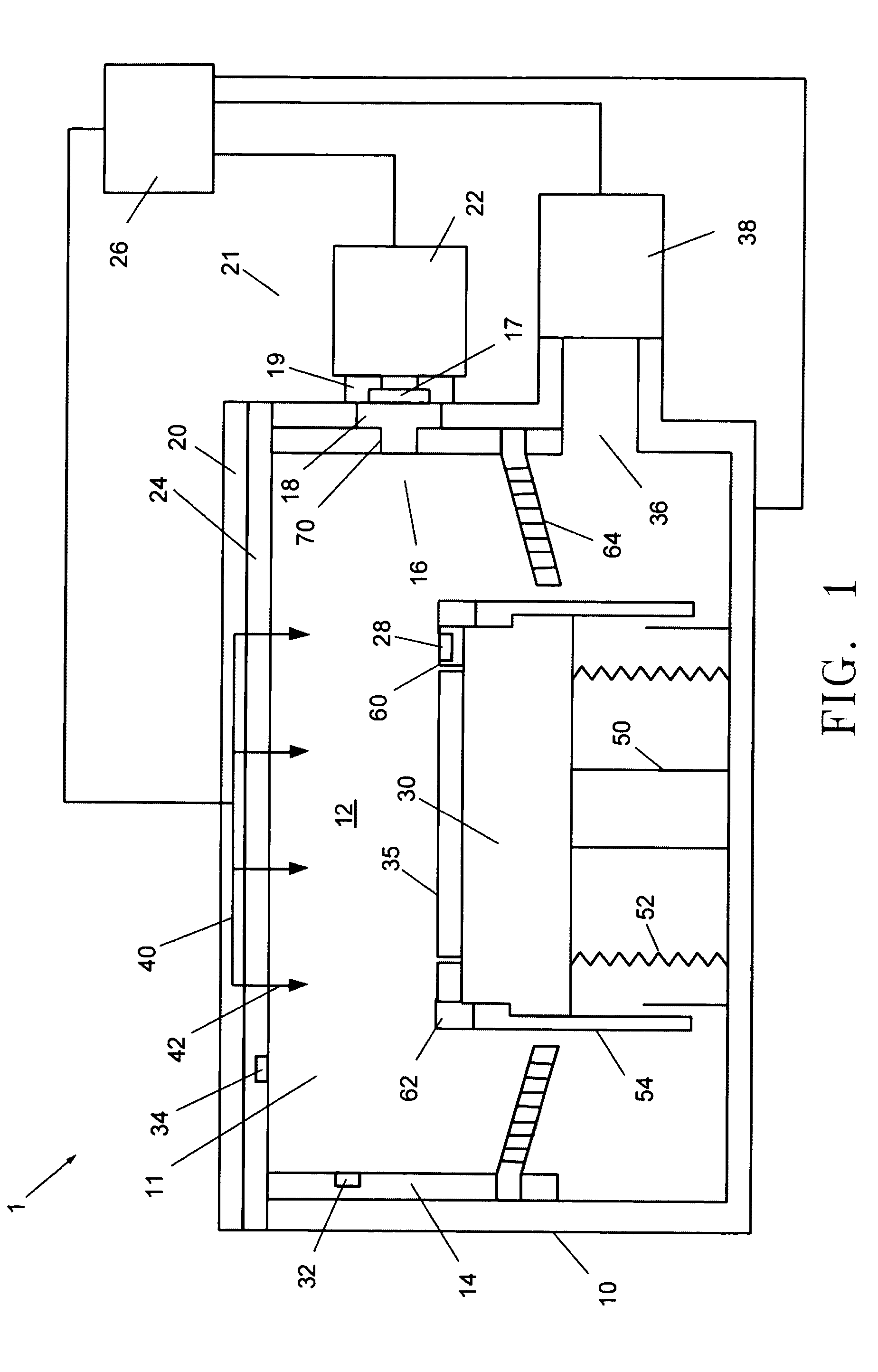
[0054]FIG. 1 shows a simplified block diagram of a plasma processing system. A plasma processing system 1 is depicted in FIG. 1 comprising a plasma processing chamber 10, an upper electrode assembly 20, an electrode plate 24, a substrate holder 30 for supporting substrate 35, and pumping duct 36 coupled to a vacuum pump 38 for providing a reduced pressure atmosphere 11 in plasma processing chamber 10. Plasma processing chamber 10 can facilitate the formation of a processing plasma in a process space 12 adjacent to substrate 35. The plasma processing system 1 can be configured to process various substrates (i.e. 200 mm substrates, 300 mm substrates, or larger).

[0055]A gas injection assembly 40 can introduce process gas 42 to the plasma processing chamber 10. The gas injection system 40 can include a showerhead (not shown), wherein the process gas 42 is supplied from a gas delivery system (not shown) to the process space 12 through a gas injection plenum (not shown), a series of baffl...


PUM

PropertyMeasurementUnit
thicknessaaaaaaaaaa
frequencyaaaaaaaaaa
frequencyaaaaaaaaaa

Abstract

A sensing device for sensing a condition of a plasma processing system component. The sensing device includes a main body configured to contain a material, an emitter contained in the main body and configured to emit light when exposed to a plasma, and a mating feature connected to the main body and configured to be mated with a receiving feature of an object in the plasma processing system such that the emitter material is exposed to a processing environment of the plasma processing system. When the emitter material is exposed to a plasma, the light emitted from the emitter can be monitored to determine at least one of material accumulation on the system component and erosion of the system component.

Description

CROSS REFERENCE TO RELATED APPLICATIONS[0001]The present invention is related to U.S. patent applications Ser. No. 10 / 331,349 filed on Dec. 31, 2002 and, Ser. No. 10 / 331,456, also filed on Dec. 31, 2002. The entire contents of each of these applications is incorporated herein by reference.FIELD OF THE INVENTION[0002]The present invention relates to plasma processing and more particularly to monitoring either material buildup or material erosion on a sensing component added to or placed close to system components in a plasma processing system using an optical monitoring system.BACKGROUND OF THE INVENTION[0003]The fabrication of integrated circuits (IC) in the semiconductor industry typically employs plasma to create and assist surface chemistry within a plasma reactor necessary to remove material from and deposit material to a substrate. In general, plasma is formed with the plasma reactor under vacuum conditions by heating electrons to energies sufficient to sustain ionizing collisi...

Claims


Application Information

Patent Timeline
Patent Type & Authority Patents(United States)
IPC IPC(8): G01J3/30G01N21/00
CPCG01N21/73
Inventor FINK, STEVEN T.
Owner TOKYO ELECTRON LTD
Why Eureka
Try Eureka