Fabrication process for integrated circuit having photodiode device

a technology of photodiode and fabrication process, which is applied in the direction of photovoltaic energy generation, electrical apparatus, basic electric elements, etc., can solve the problems of low capacitance of the junction, low doping gradient at the junction, and difficult to produce a good photodiode, so as to reduce the doping gradient, increase the capacitance associated with the junction, and extend the space charge region large

Inactive Publication Date: 2006-09-26
STMICROELECTRONICS SRL
View PDF5 Cites 0 Cited by
  • Summary
  • Abstract
  • Description
  • Claims
  • Application Information

AI Technical Summary

Benefits of technology

[0008]Another object of the present invention is to reduce the doping gradient at the junction so as to obtain a large extension of the space charge region even for low applied voltages.
[0009]Yet another object of the present invention is to increase the capacitance associated with the junction, while neither inc

Problems solved by technology

To produce a good photodiode is tricky.
This means that the doping gradient at the junction is low.
However, if the doping gradient is low, the capacitance of the junction is

Method used


Image

  • Fabrication process for integrated circuit having photodiode device
  • Fabrication process for integrated circuit having photodiode device
  • Fabrication process for integrated circuit having photodiode device

Examples


Embodiment Construction

[0015]Preferred embodiments of the present invention will be described in detail hereinbelow with reference to the attached drawings.

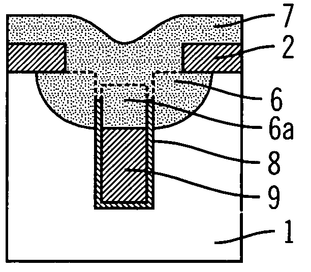
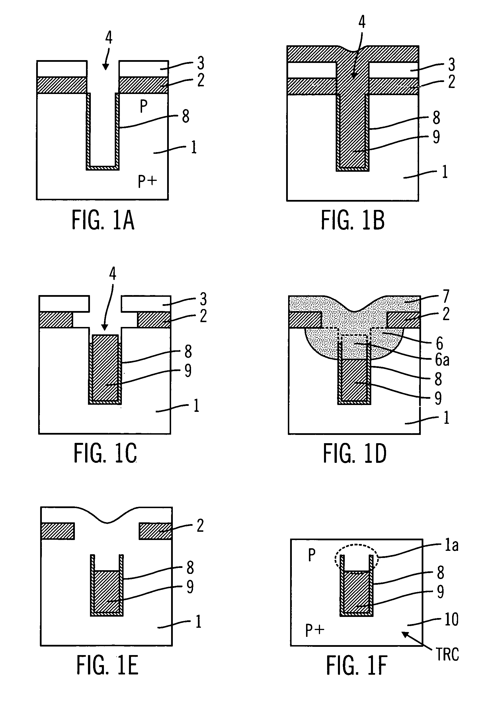
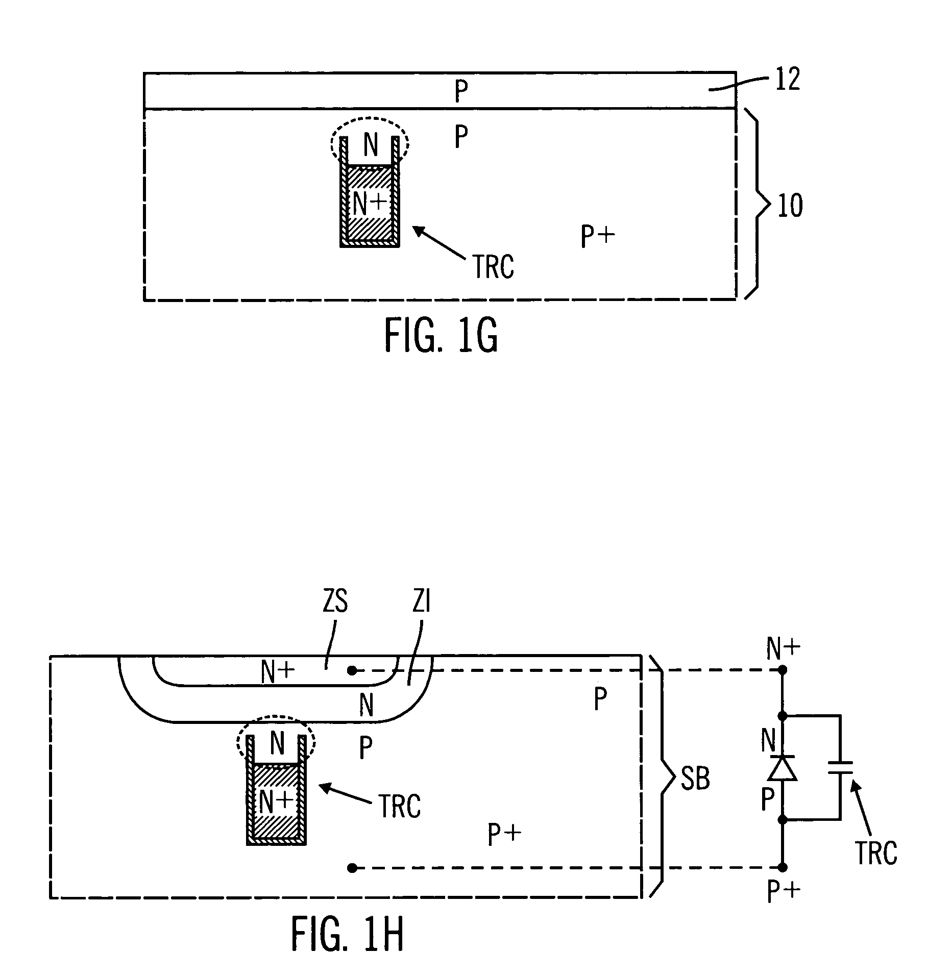
[0016]One preferred embodiment of the present invention provides an integrated circuit that includes a substrate incorporating a semiconductor device of the photodiode type having a p-n junction. The device includes a capacitive trench buried in the substrate and connected in parallel with the junction.

[0017]Preferably, the junction has a low doping level or a low doping gradient, so that the length of the space charge region is greater than 1 micron even for low reverse voltages (for example, of less than 1 volt). For example, this can be achieved by a doping of less than 1015 at / cm3 in the case of a sharp junction with low doping on only one side or else by a doping gradient of less than 1020 at / cm3 in the case of a junction with linear doping. Moreover, this parameter is decorrelated with the capacitance parameter. In this regard, the capacitance as...


PUM


Abstract

An integrated circuit is provided that includes a substrate incorporating a semiconductor photodiode device having a p-n junction. The photodiode device includes at least one capacitive trench buried in the substrate and connected in parallel with the junction. In a preferred embodiment, the substrate is formed from silicon, and the capacitive trench includes an internal doped silicon region partially enveloped by an insulating wall that laterally separates the internal region from the substrate. Also provided is a method for fabricating an integrated circuit including a substrate that incorporates a semiconductor photodiode device having a p-n junction.

Description

CROSS-REFERENCE TO RELATED APPLICATIONS[0001]This application is a divisional of application Ser. No. 10 / 044,286, filed Jan. 11, 2002, now U.S. Pat. No. 6,670,657, which is based upon and claims priority from prior French Patent Application No. 01-00420, filed Jan. 12, 2001, the entire disclosure of which is herein incorporated by reference.BACKGROUND OF THE INVENTION[0002]1. Field of the Invention[0003]The present invention relates to integrated circuits, and more specifically to integrated circuits that include photodiode-type semiconductor devices.[0004]2. Description of Related Art[0005]To produce a good photodiode is tricky. This is because it has to be sensitive to light and only the space charge region of the junction is capable of collecting the carriers generated by the light excitation, because of the electric field existing in this region. Now, a photodiode is more sensitive the larger the space charge region. This means that the doping gradient at the junction is low. Ho...

Claims


Application Information

Patent Timeline
IPC IPC(8): H01L21/00H01L27/144H01L27/146H01L31/0352
CPCH01L27/1443H01L27/14603H01L31/03529H01L27/14643Y02E10/50
Inventor MENUT, OLIVIERGRIS, YVON
Owner STMICROELECTRONICS SRL
Why Eureka
Try Eureka