Tunable wavelength laser

a wavelength laser and wavelength technology, applied in semiconductor lasers, semiconductor laser arrangements, active medium materials, etc., can solve the problems of complicated wavelength control, and large number of parts, and achieve wide wavelength variation range and high photooutput

Inactive Publication Date: 2006-09-26
FUJITSU LTD
View PDF7 Cites 47 Cited by
  • Summary
  • Abstract
  • Description
  • Claims
  • Application Information

AI Technical Summary

Benefits of technology

[0024]An object of the present invention is to provide a photosemiconductor device which can have a wide wavelength variation range and can provide high photooutputs.

Problems solved by technology

The large number of the parts complicates the inventory control.
However, these laser light sources have disadvantages such that they cannot provide larger photooutputs when they vary the wavelength, the range in which the wavelength can be continuously varied is as narrow as some nanometers, which makes the wavelength control complicated, and the mode hopping causes the discontinuous wavelength variation, etc.
However, the TTG-DFB laser as well as the other lasers has the disadvantage that the injection of current in the wavelength tuning layer for varying a wavelength to a shorter wavelength increases the internal loss of the laser, causing large decrease of photooutput.
However, this causes, on the other hand, the active layer temperature, i.e., the element temperature increase, causing the opposite effect of shifting the oscillation wavelength to a longer wavelength.
Furthermore, the wavelength shift due to the temperature increase must be again controlled by the wavelength tuning current, which complicates the wavelength variation method.
However, it cannot be said that the control disclosed in Japanese Patent Application Unexamined Publication No.
The integrated structure is not of optical elements having gains, and is not expected to much increase the photooutput.
As described above, the above-described photosemiconductor devices cannot realize high photooutputs although having wide wavelength variation ranges.
Accordingly, when the TTG-LD is integrated with other elements, such as an optical waveguide, etc., on one and the same substrate, disadvantages, such as characteristic deterioration, etc., will take place.

Method used


Image

  • Tunable wavelength laser
  • Tunable wavelength laser
  • Tunable wavelength laser

Examples


first embodiment

[0078][A First Embodiment]

[0079]The photosemiconductor device and the method for fabricating the photosemiconductor device according to a first embodiment of the present invention will be explained with reference to FIGS. 1A–1C, 2A–2D and 3A–3D.

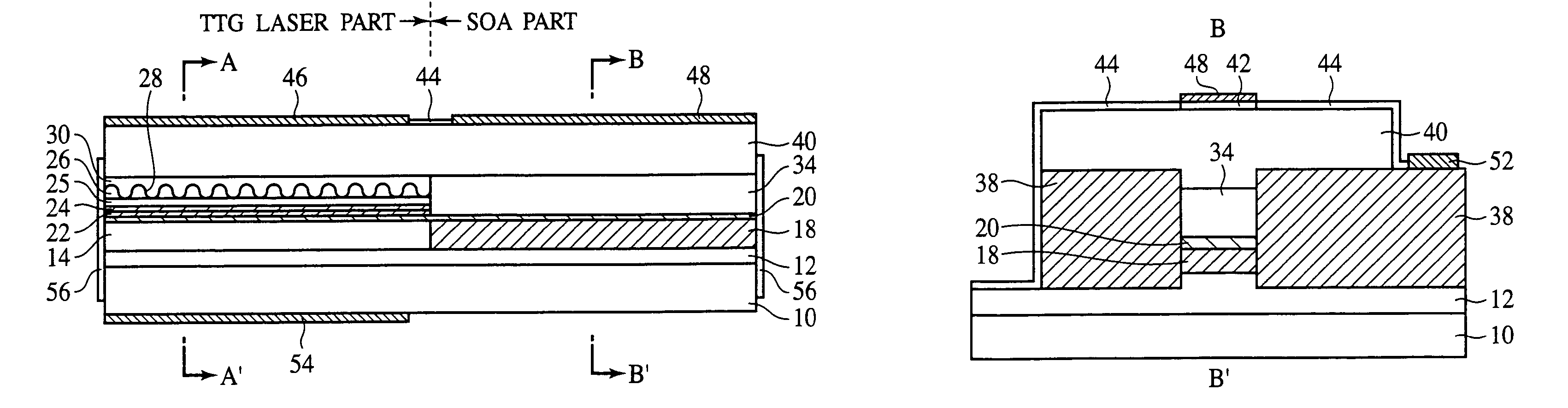
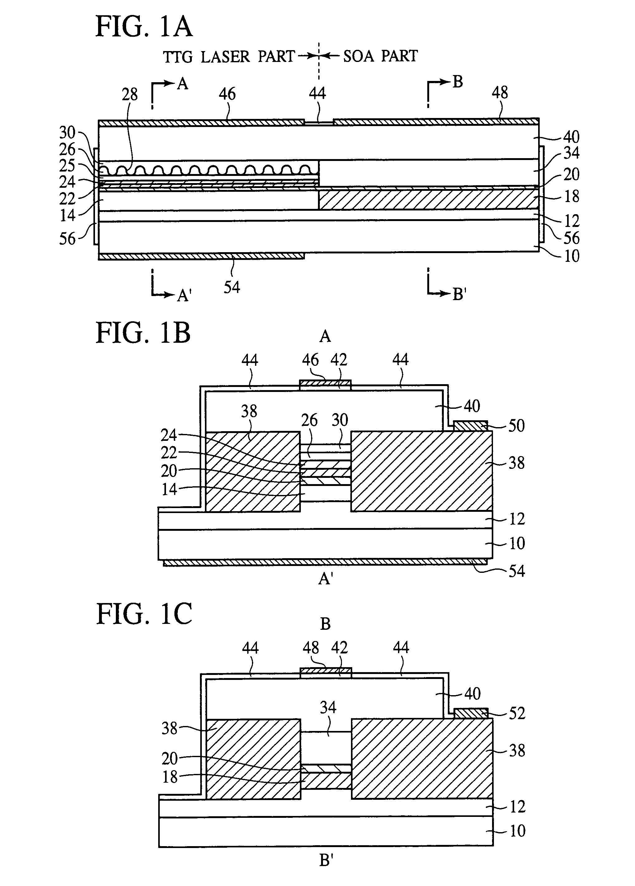
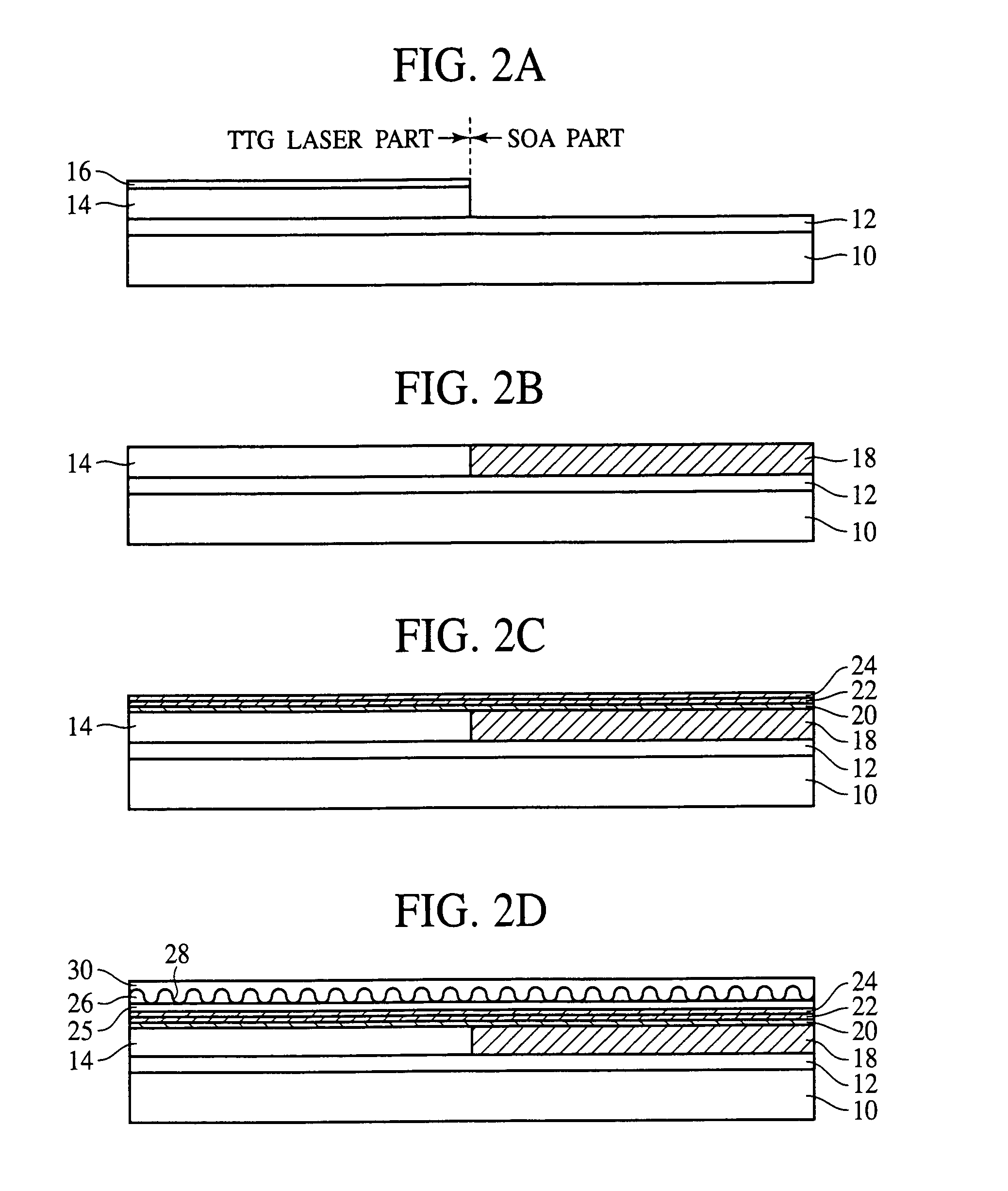
[0080]FIGS. 1A–1C are diagrammatic sectional views of the photosemiconductor device according to the present embodiment, which show the structure thereof. FIGS. 2A–2D and 3A–3D are sectional views of the photosemiconductor device according to the present embodiment in the steps of the method for fabricating the photosemiconductor device, which show the method.

[0081]First, the structure of the photosemiconductor device according to the present embodiment will be explained with reference to FIGS. 1A–1C. FIG. 1A is a diagrammatic sectional of the mesa stripe along the extension thereof. FIG. 1B is a diagrammatic sectional view of the TTG laser part along the line A–A′ in FIG. 1A. FIG. 1C is a diagrammatic sectional view of the SOA part along the...

second embodiment

[0126][A Second Embodiment]

[0127]The photosemiconductor device and the method for fabricating the photosemiconductor device according to a second embodiment of the present invention will be explained with reference to FIGS. 4A–4C and 5A–5D. The same members of the photosemiconductor device according to the present embodiment as those of the photosemiconductor device and the method for fabricating the photosemiconductor device according to the first embodiment shown in FIGS. 1A–1C, 2A–2D and 3A–3D are represented by the same reference numbers not to repeat or to simplify their explanation.

[0128]FIGS. 4A–4C are diagrammatic sectional views of the photosemiconductor device according to the present embodiment, which show a structure thereof. FIGS. 5A–5D are sectional views of the photosemiconductor device according to the present embodiment in the steps of the method for fabricating the same, which show the method.

[0129]First, the structure of the photosemiconductor device according to ...

third embodiment

[0152][A Third Embodiment]

[0153]The photosemiconductor device and the method for fabricating the photosemiconductor device according to a third embodiment of the present invention will be explained with reference to FIG. 6. The same reference numbers of the present embodiment as those of the photosemiconductor device and the method for fabricating the photosemiconductor device according to the first and the second embodiments shown in FIGS. 1A–1C, 2A–2D, 3A–3D, 4A–4C and 5A–5D are represented by the same reference numbers not to repeat or to simplify their explanation.

[0154]FIG. 6 is a diagrammatic sectional view of the photosemiconductor device according to the present embodiment, which shows the structure thereof.

[0155]The basic structure of the photosemiconductor device according to the present embodiment is the same as that of the photosemiconductor device according to the first embodiment shown in FIGS. 1A–1C. The present embodiment is different from the photosemiconductor devi...


PUM


Abstract

A light oscillation part including an active layer for generating light by current injection, a tuning layer with an intermediate layer formed between the active layer and the tuning layer, for varying an oscillation wavelength by current injection and a diffraction grating formed near the active layer and the tuning layer, and a light amplification part including an active layer for amplifying light by current injection are formed on a semiconductor substrate. Light oscillation elements having wide wavelength variation ranges and the light amplification are integrated on a semiconductor substrate, whereby wide wavelength variation ranges can be obtained and the output light can be much increased.

Description

CROSS-REFERENCE TO APPLICATIONS[0001]This application is based upon and claims priorities of Japanese Patent Application No. 2002-306832, filed on Oct. 22, 2002, Japanese Patent Application No. 2002-355271, filed on Dec. 6, 2002, and Japanese Patent Application No. 2003-135908, filed on May 14, 2003, the contents being incorporated herein by reference.BACKGROUND OF THE INVENTION[0002]1. Field of the Invention[0003]The present invention relates to a photosemiconductor device, a method for fabricating the photosemiconductor device and a method for driving the photosemiconductor device, more specifically a photosemicondcutor device which has a wide wavelength variation range and can provide high photooutputs, a method for driving the photosemiconductor device, and a photosemiconductor device including a tunable twin guide laser and an optical waveguide integrated on one and the same substrate and a method for fabricating the photosemiconductor device.[0004]2. Description of the Related...

Claims


Application Information

Patent Timeline
Patent Type & Authority Patents(United States)
IPC IPC(8): H01L29/74H01L31/111H01S3/10H01S3/17H01S5/026H01L27/15H01S5/028H01S5/042H01S5/06H01S5/062H01S5/0625H01S5/12H01S5/22H01S5/227H01S5/323H01S5/40
CPCH01S5/0607H01S5/06206H01S5/06258H01S5/227H01S5/026H01S2301/173H01S5/028H01S5/042H01S5/0425H01S5/1014H01S5/2206H01S5/32333H01S5/4012H01S5/4087H01S5/0265H01S5/04252H01S5/04256
Inventor HAYAKAWA, AKINORISATO, YOSHIHIROMORITO, KENSEKINE, NORIHIKO
Owner FUJITSU LTD
Why Eureka
Try Eureka