Semiconductor constructions comprising aluminum oxide and metal oxide dielectric materials

a technology of dielectric materials and semiconductors, applied in semiconductor devices, capacitors, electrical devices, etc., can solve problems such as unfavorable and unexpected problems, and affecting the performance of semiconductor devices

Inactive Publication Date: 2006-10-03
MICRON TECH INC
View PDF5 Cites 10 Cited by
  • Summary
  • Abstract
  • Description
  • Claims
  • Application Information

AI Technical Summary

Problems solved by technology

It is frequently challenging to utilize the compositions in semiconductor constructions, in that the compositions can create undesired and unexpected problems.

Method used


Image

  • Semiconductor constructions comprising aluminum oxide and metal oxide dielectric materials
  • Semiconductor constructions comprising aluminum oxide and metal oxide dielectric materials
  • Semiconductor constructions comprising aluminum oxide and metal oxide dielectric materials

Examples


Embodiment Construction

[0017]This disclosure of the invention is submitted in furtherance of the constitutional purposes of the U.S. Patent Laws “to promote the progress of science and useful arts” (Article 1, Section 8).

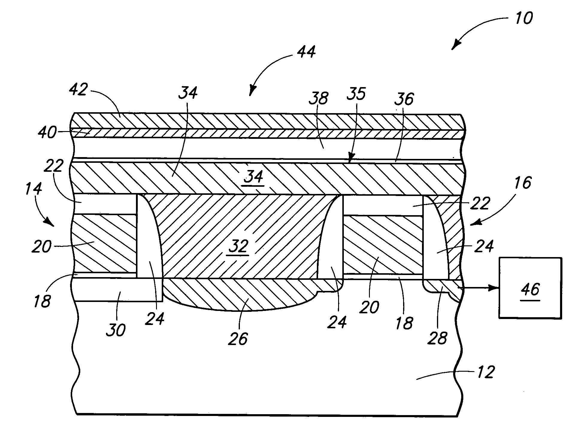
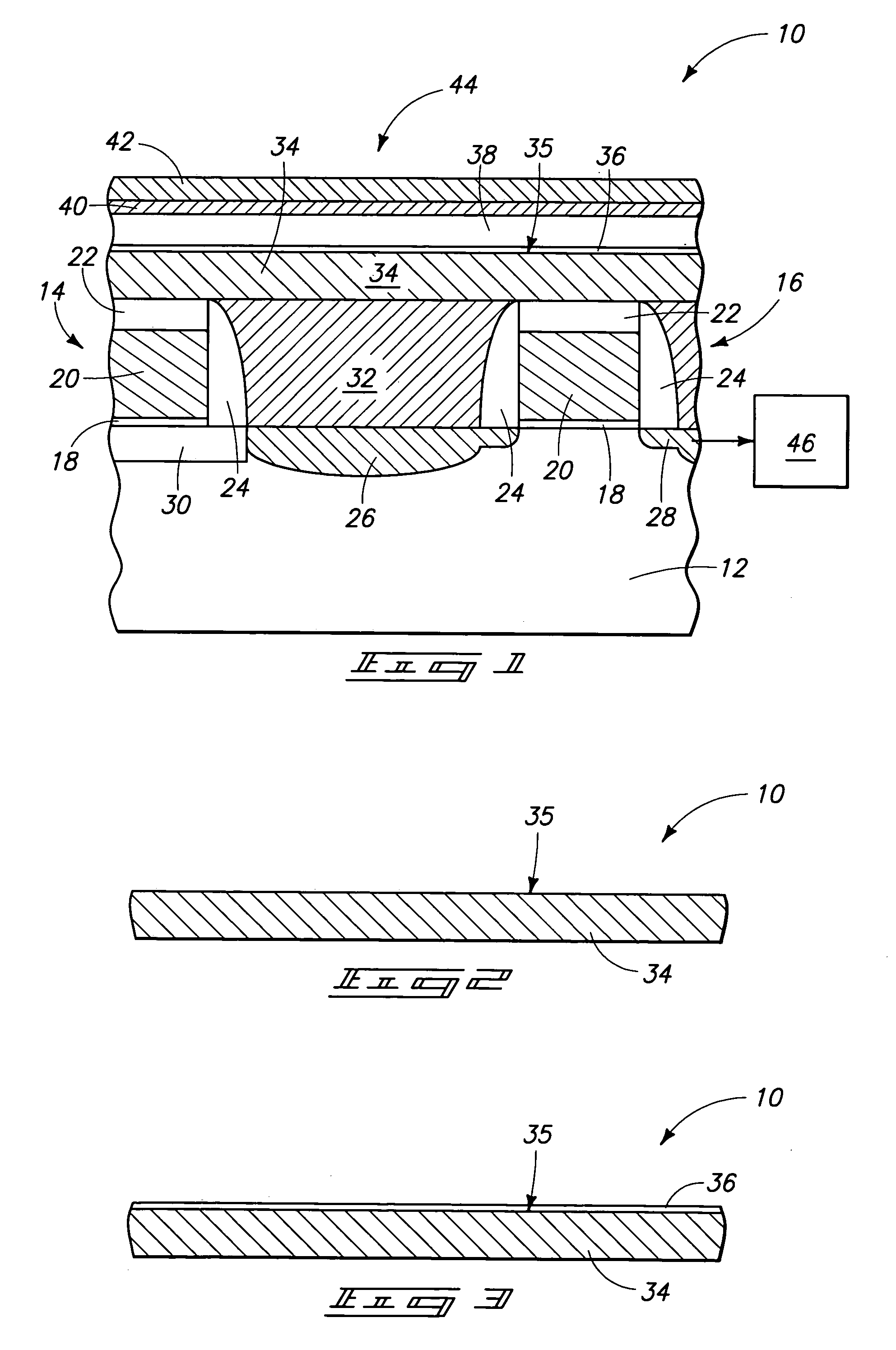
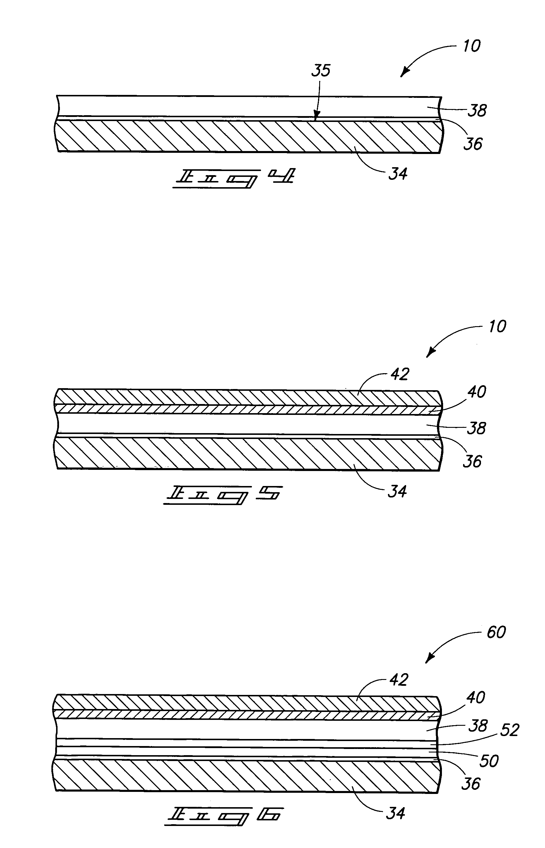
[0018]Among the compositions which have been developed for utilizationas capacitor dielectric materials are metal oxides, such as, for example, aluminum oxide, hafnium oxide, titanium oxide, zirconium oxide and tantalum oxide. Hafnium oxide, tantalum oxide and zirconium oxide can be particularly desired, in that such oxides have relatively high dielectric constants. However, one aspect of the invention is a recognition that if hafnium oxide, tantalum oxide and / or zirconium oxide is provided directly against a conductively-doped semiconductor material (such as, for example, conductively-doped silicon), current leakage can occur between the dielectric material and the conductively-doped semiconductor material. If an appropriate intervening (barrier) material is provided between the conducti...


PUM

PropertyMeasurementUnit
semiconductoraaaaaaaaaa
electrically conductiveaaaaaaaaaa
insulatingaaaaaaaaaa

Abstract

The invention includes constructions having two dielectric layers over a conductively-doped semiconductive material. One of the dielectric layers contains aluminum oxide, and the other contains a metal oxide other than aluminum oxide (such metal oxide can be, for example, one or more of hafnium oxide, tantalum oxide, titanium oxide and zirconium oxide). The layer containing aluminum oxide is between the layer containing metal oxide and the conductively-doped semiconductive material. The invention includes capacitor devices having one electrode containing conductively-doped silicon and another electrode containing one or more metals and / or metal compounds. At least two dielectric layers are formed between the two capacitor electrodes, with one of the dielectric layers containing aluminum oxide and the other containing a metal oxide other than aluminum oxide. The invention also includes methods of forming capacitor constructions.

Description

TECHNICAL FIELD[0001]The invention pertains to devices comprising aluminum oxide and metal oxide dielectric materials, and in particular aspects pertains to capacitor constructions. The invention also pertains to methods of forming capacitor constructions.BACKGROUND OF THE INVENTION[0002]Dielectric materials are utilized in numerous devices associated with semiconductor constructions, including, for example, capacitors. A continuing goal in semiconductor device fabrication is to decrease the footprint consumed by the devices while maintaining, and preferably improving, performance of the devices. In an effort to achieve such goal, various new compositions have been developed which can be incorporated into integrated circuit device constructions. It is frequently challenging to utilize the compositions in semiconductor constructions, in that the compositions can create undesired and unexpected problems.[0003]In the specific case of capacitor constructions, it is frequently desired to...

Claims


Application Information

Patent Timeline
Patent Type & Authority Patents(United States)
IPC IPC(8): H01L29/72H01L21/00H01L21/02H01L21/316H01L21/8242
CPCH01L28/40H01L28/56H01L21/31616H01L21/31637H01L21/31641H01L21/31645H01L21/022H01L21/02175H01L21/02178
Inventor BHAT, VISHWANATHGEALY, F. DANIELSRIVIDYA, CANCHEEPURAM V.
Owner MICRON TECH INC
Why Eureka
Try Eureka