Optical waveguide structure

a waveguide and optical waveguide technology, applied in the field of optical devices, can solve the problems of difficult to produce integrated optical circuits which are comparably small, formation of allowed and forbidden energy states, and difficult to produce integrated optical circuits, etc., to achieve the effect of improving the influence of the photonic band structure, easy fabrication, and increasing fabrication tolerances

Inactive Publication Date: 2006-10-03
QUANTUM NIL LTD +1
View PDF5 Cites 14 Cited by
  • Summary
  • Abstract
  • Description
  • Claims
  • Application Information

AI Technical Summary

Benefits of technology

[0014]By forming sub-regions in the cladding layer and not in the core layer, the large losses of light in the vertical direction can be substantially reduced.
[0027]In-filling sub-regions with a material having a higher refractive index than the effective mode index means that the dimensions required for the lattice pitch to produce a bandgap at a wavelength typically used, for example for telecommunications, can be much larger than in conventional photonic crystals. Furthermore, the cladding PC with sub-regions in-filled with higher refractive index material possesses a complete bandgap when embedded in a low index material (such as a glassy core material). Fabrication tolerances can be greatly increased because the sub-regions can be spaced further apart and each sub-region can be larger. Consequently, the waveguide of the present invention can easily be fabricated using conventional lithography. Air filled sub-regions typically require much higher precision lithography.

Problems solved by technology

However, it has been difficult to produce integrated optical circuits which are comparably small, primarily due to the difficulty in producing waveguides which can include tight bends without large signal losses.
It has also been difficult to produce integrated optical circuits including signal processing devices which can be easily coupled to current optical fibres, owing to a difference in the refractive index of the material used for optical fibres and those materials typically used for integrated optical devices, whilst still maintaining compact sizes.
This interaction results in the formation of allowed and forbidden energy states.
However, it has been found that photonic crystal devices suffer from large losses, mainly due to the escape of light from the waveguide in a vertical direction.
This makes it difficult to couple light into the waveguides from existing optical fibres, which typically have a core having a much lower refractive index.
This problem necessitates complicated, lossy mode coupling devices.

Method used


Image

  • Optical waveguide structure
  • Optical waveguide structure
  • Optical waveguide structure

Examples


first embodiment

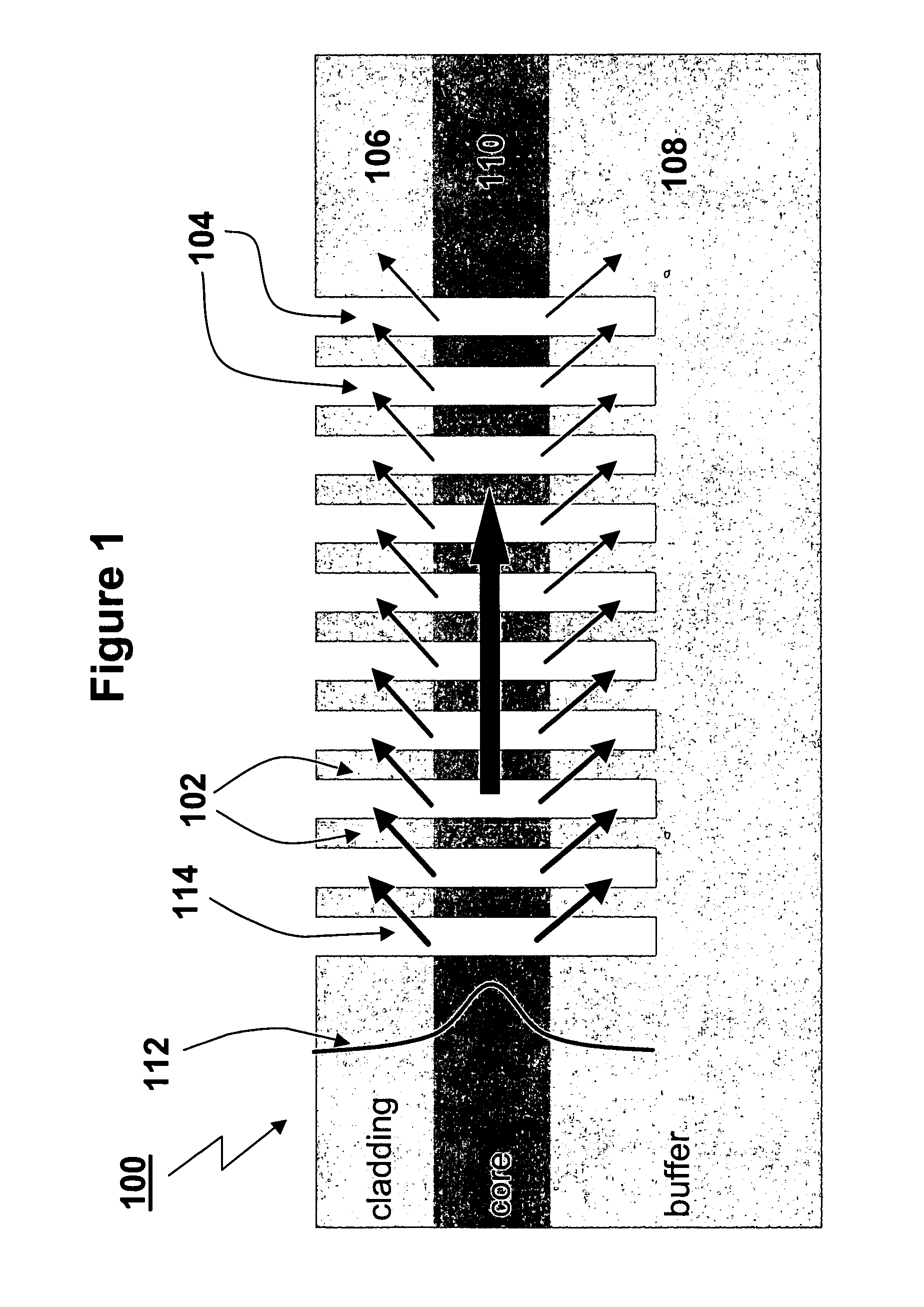
[0080]FIG. 5 shows the invention. Here, a planar waveguide structure 500 includes a substrate 512, a buffer layer 508, a core layer 510 and a cladding layer 506. The core 510 of the waveguide structure is disposed between the cladding layer 506 and the buffer layer 508. An array of mutually parallel trenches 502 is formed in the cladding layer 506, the trenches 502 being aligned perpendicularly to the direction of propagation of an optical signal through the waveguide 500. The trenches (or slots) 502 are air-filled.

second embodiment

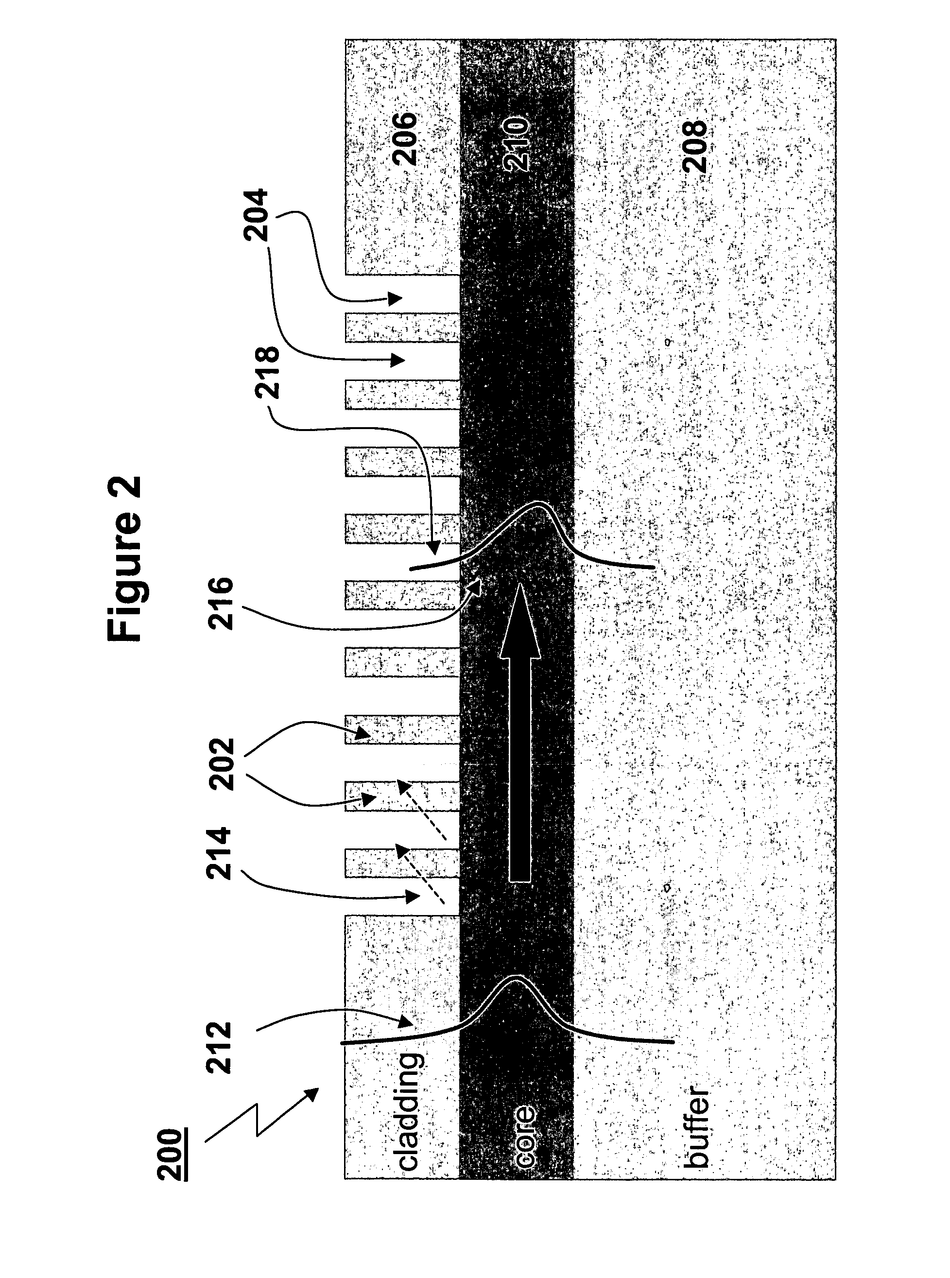
[0081]FIG. 6 shows the invention. Here, a planar waveguide structure 600 includes a substrate 612, a buffer layer 608, a core layer 610 and a cladding layer 606. The core 610 of the waveguide structure is disposed between the cladding layer 606 and the buffer layer 608. An array of mutually parallel trenches 602 is formed in the cladding layer 606, the trenches 602 being aligned perpendicularly to the direction of propagation of an optical signal through the waveguide 600. The trenches (or slots) 502 are formed of a filler material having a higher dielectric constant than air.

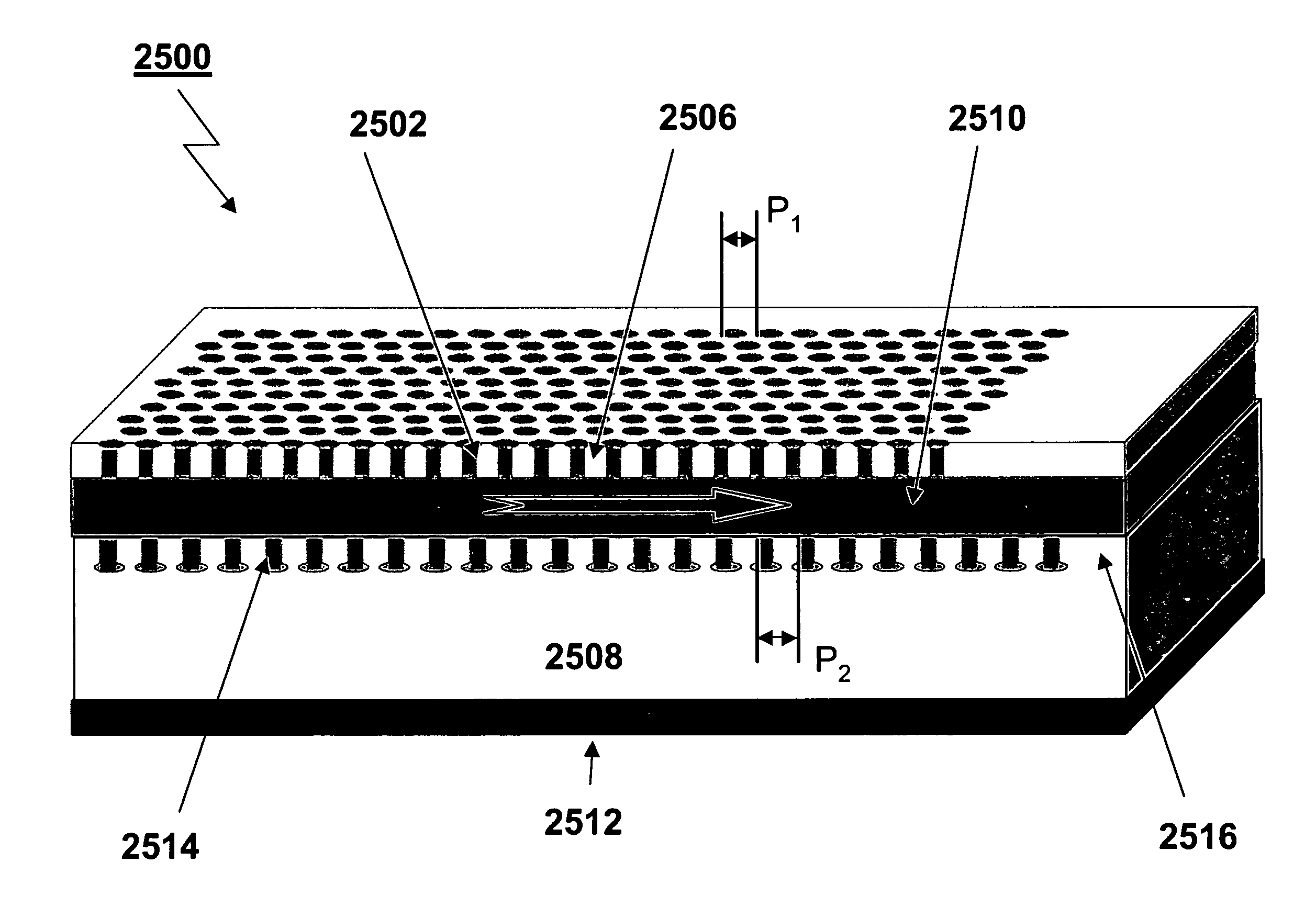
[0082]FIG. 7 shows a third embodiment of the invention. Similarly to the first embodiment, FIG. 7 shows a planar waveguide structure 700 including a substrate 712, a buffer layer 708, a core layer 710 and a cladding layer 706. The core 710 of the waveguide structure is disposed between the cladding layer 706 and the buffer layer 708. An array of holes or rods 702 is formed in the cladding layer 706. The holes o...

sixth embodiment

[0086]FIG. 11 shows the invention. Here, a planar waveguide structure 1100 includes a substrate 1112, a buffer layer 1108, a core layer 1110 and a cladding layer 1106. The core 1110 of the waveguide structure is disposed between the cladding layer 1106 and the buffer layer 1108. An array of mutually parallel trenches 1102 is formed In the cladding layer 1106, the trenches 1102 being aligned perpendicularly to the direction of propagation of an optical signal through the waveguide 1100. The trenches (or slots) 1102 are formed of a filler material having a higher dielectric constant than air. In this embodiment, a further array of mutually parallel trenches 1114 is formed in an upper portion 1116 of the buffer layer 1108. Again the trenches 1114 are aligned perpendicularly to the direction of propagation of an optical signal and again the trenches (or slots) 1114 are formed of a filler material having a higher dielectric constant than air.

[0087]FIG. 12 shows a seventh embodiment of th...


PUM


Abstract

A waveguide structure (200) according to the invention comprises a core layer (210), a cladding layer (206) and a buffer layer (208). Sub-regions (204) are formed in the cladding layer (206) but not in the core layer (210). In one dimensional applications the sub-regions are slots: in two dimensional applications the sub-regions are rods. The rods or slots may be air-filled or filled with an in-fill material, (e.g. Si). The in-fill material, if present, enhances the contrast in dielectric constant between sub-regions (204) and the core layer (210).Sub-regions (204) may furthermore be formed in the portion of the buffer layer neighbouring the core layer. Slots or rods in the buffer may be air-filled or filled by an in-fill material.Substantially complete confinement of the mode in the core can be assured while still maintaining the ability to interact with the field within the photonic band structure region. Rather than perturb the majority of the field (which is confined in the core), it is possible to interact with the evanescent field in the cladding layer (or the buffer layer) without substantially affecting mode confinement.

Description

FIELD OF THE INVENTION[0001]The present invention relates to the field of optical devices and in particular but not exclusively to waveguide structures in Integrated optical circuits.BACKGROUND TO THE INVENTION[0002]It is increasingly recognised that integrated optical circuits have a number of advantages over electrical circuits. However, it has been difficult to produce integrated optical circuits which are comparably small, primarily due to the difficulty in producing waveguides which can include tight bends without large signal losses. It has also been difficult to produce integrated optical circuits including signal processing devices which can be easily coupled to current optical fibres, owing to a difference in the refractive index of the material used for optical fibres and those materials typically used for integrated optical devices, whilst still maintaining compact sizes.[0003]Optical signals may be resonantly confined and manipulated using structures whose periodicity is...

Claims


Application Information

Patent Timeline
Patent Type & Authority Patents(United States)
IPC IPC(8): G02B6/10G02B6/122
CPCB82Y20/00G02B6/1225
Inventor ZOOROB, MAJDCHARLTON, MARTINPARKER, GREG
Owner QUANTUM NIL LTD
Why Eureka
Try Eureka