Methods of forming patterned photoresist layers over semiconductor substrates

a technology of photoresist and semiconductor substrate, which is applied in the direction of photomechanical treatment, photomechanical instruments, photosensitive materials, etc., can solve the problems of adversely affecting the final pattern developed pattern, adversely affecting the adhesion or desired control of the final pattern produced in the photoresist, and affecting the footing of the photoresist. , to achieve the effect of reducing the footing of the photoresis

Active Publication Date: 2006-10-10
MICRON TECH INC
View PDF83 Cites 6 Cited by
  • Summary
  • Abstract
  • Description
  • Claims
  • Application Information

AI Technical Summary

Benefits of technology

[0010]In one implementation, a method of forming a patterned photoresist layer over a semiconductor substrate includes forming a porous antireflective coating over a semiconductor substrate. A photoresist base-widening fluid is provided within pores of the porous antireflective coating. A positive photoresist is formed over the porous antireflective coating having the fluid therein. The positive photoresist is patterned and developed to form a patterned photoresist layer, with the fluid within the pores being effective to widen a base of the patterned photoresist adjacent the antireflective coating than would otherwise occur in the absence of the fluid within the pores.

Problems solved by technology

A difficulty which can be encountered during photolithographic processing is that the radiation utilized to pattern the photoresist can be reflected from the underlying layer or layers to cause various constructive and destructive interference patterns to occur.
This can adversely affect the pattern ultimately developed in the photoresist.
For example, material at the outer surface of the antireflective coating materials can migrate into the photoresist, and / or the photoresist can interact with material on the outer surface of the antireflective coating which can, one or both, adversely affect adherence or desired control in the ultimate pattern produced in the photoresist.
Further in some instances, the patterned photoresist can tend to recess in at the bottom / bases of the individual masking blocks which can lead to collapse / toppling of portions of the mask and / or less than desired transfer of the mask pattern to underlying layers.

Method used


Image

  • Methods of forming patterned photoresist layers over semiconductor substrates
  • Methods of forming patterned photoresist layers over semiconductor substrates
  • Methods of forming patterned photoresist layers over semiconductor substrates

Examples


Embodiment Construction

[0024]This disclosure of the invention is submitted in furtherance of the constitutional purposes of the U.S. Patent Laws “to promote the progress of science and useful arts” (Article 1, Section 8).

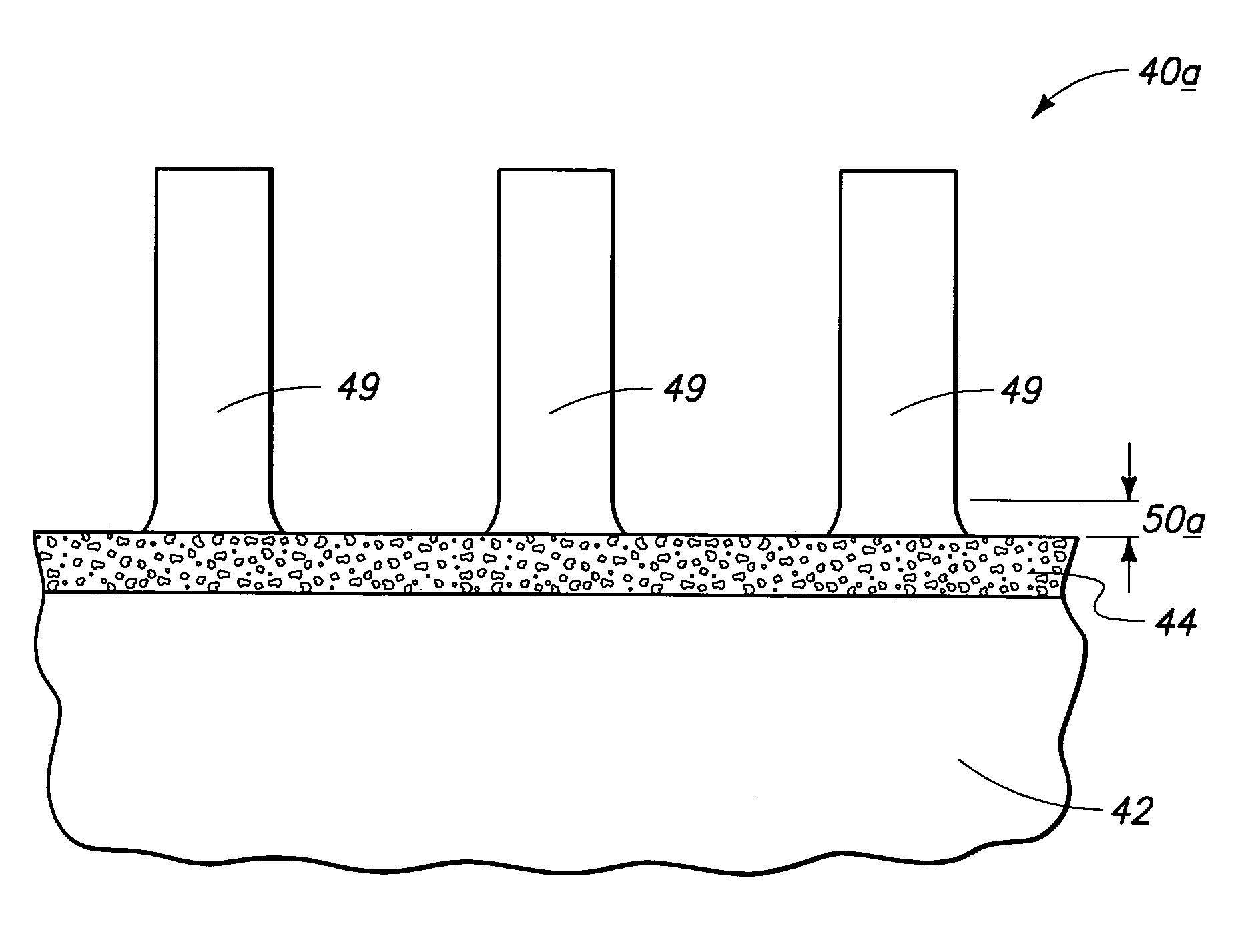
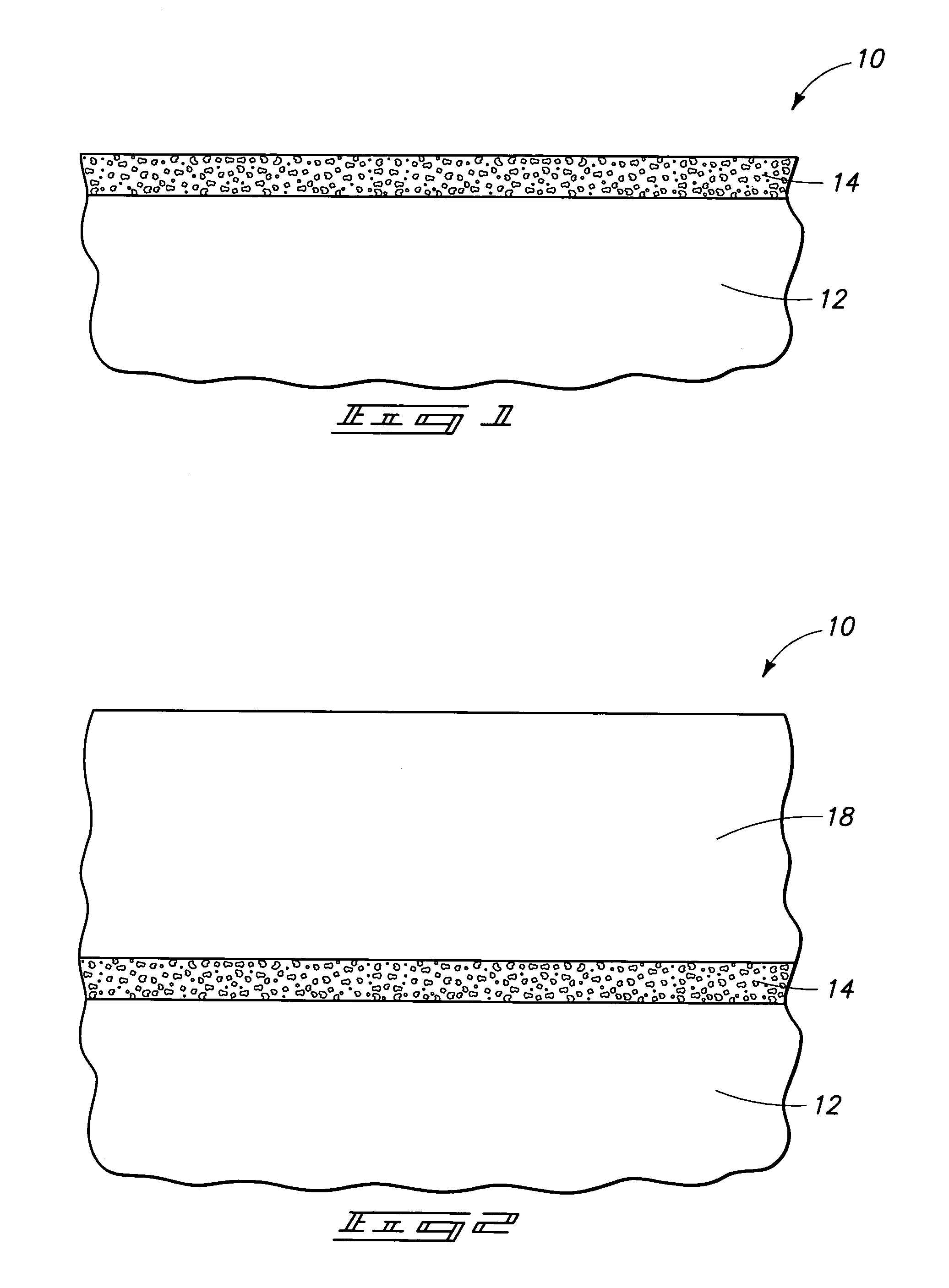
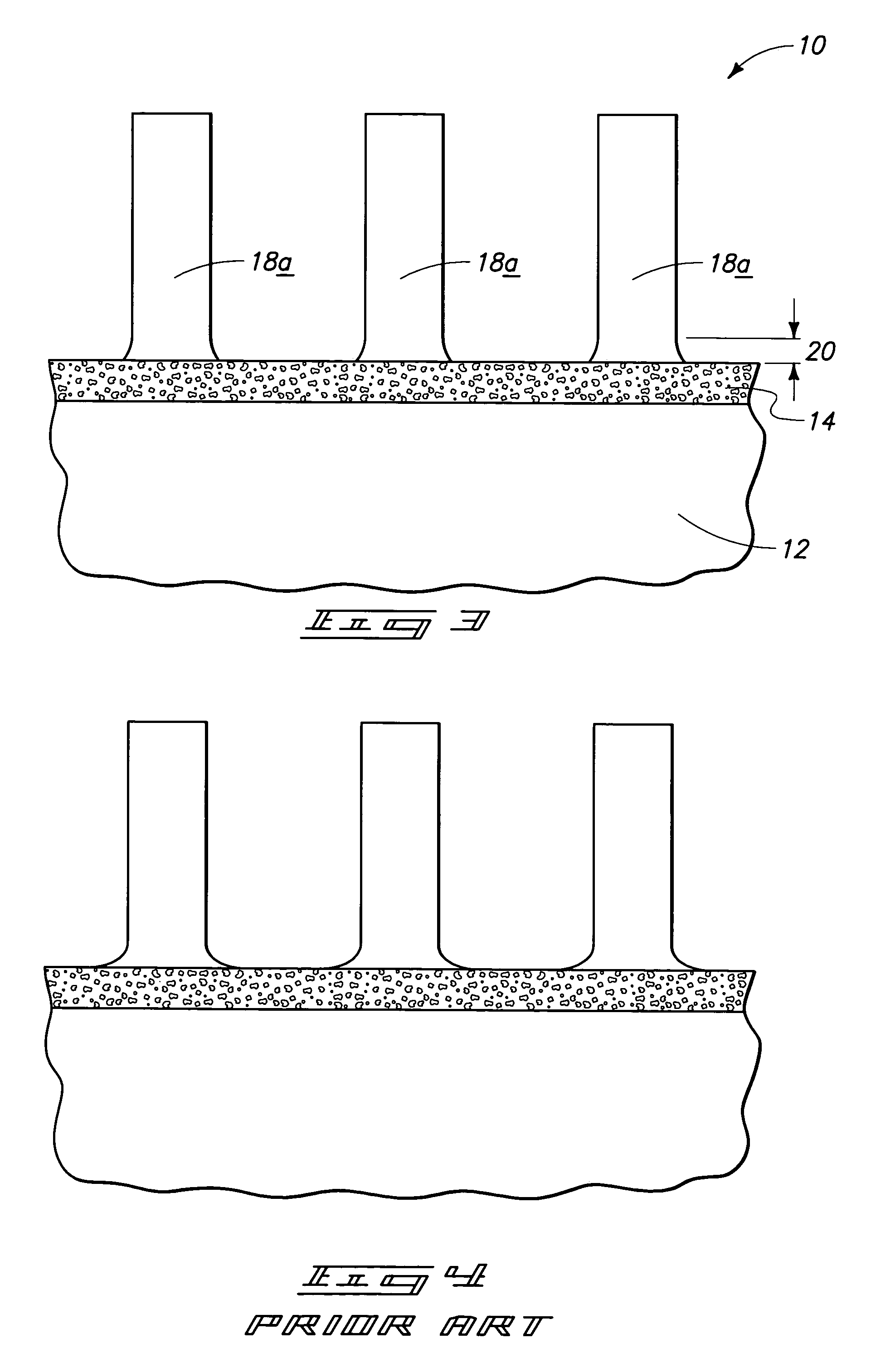
[0025]A method of forming a patterned photoresist layer over a semiconductor substrate is described initially with reference to an exemplary embodiment as depicted in FIGS. 1–3. Referring initially to FIG. 1, a wafer fragment 10 comprises a semiconductor substrate 12. In the context of this document, the term “semiconductor substrate” or “semiconductive substrate” is defined to mean any construction comprising semiconductive material, including, but not limited to, bulk semiconductive materials such as a semiconductive wafer (either alone or in assemblies comprising other materials thereon), and semiconductive material layers (either alone or in assemblies comprising other materials). The term “substrate” refers to any supporting structure, including, but not limited to, the semiconductiv...


PUM

PropertyMeasurementUnit
thicknessaaaaaaaaaa
thicknessaaaaaaaaaa
pKaaaaaaaaaaa

Abstract

This invention includes methods of forming patterned photoresist layers over semiconductor substrates. In one implementation, a porous antireflective coating is formed over a semiconductor substrate. A photoresist footer-reducing fluid is provided within pores of the porous antireflective coating. A positive photoresist is formed over the porous antireflective coating having the fluid therein. The positive photoresist is patterned and developed to form a patterned photoresist layer, with the fluid within the pores being effective to reduce photoresist footing in the patterned photoresist layer than would otherwise occur in the absence of the fluid within the pores. Other aspects and implementations are contemplated.

Description

TECHNICAL FIELD[0001]This invention relates to methods of forming patterned photoresist layers over semiconductor substrates.BACKGROUND OF THE INVENTION[0002]A continuing goal in semiconductor processing is increased miniaturization while maintaining high performance. Modern semiconductor processes are still heavily reliant on photolithography when fabricating semiconductor circuitry to achieve this goal.[0003]Photolithography is a commonly-used method for patterning features during semiconductor processing. A radiation-sensitive material (i.e., photoresist) is formed over a substrate which is ultimately to be patterned, for example by etching or ion implanting. The photoresist is subsequently subjected to radiation which modifies the solubility of the impacted versus the unimpacted regions in a suitable developer solution. Accordingly, the radiation is provided in a desired pattern so that some portions of the photoresist are impacted by the radiation while other portions of the ph...

Claims


Application Information

Patent Timeline
Patent Type & Authority Patents(United States)
IPC IPC(8): H01L21/31G03F7/09H01L21/027H01L21/469H01L21/4763H01L21/768
CPCG03F7/091H01L21/0276
Inventor BLALOCK, GUY T.SANDHU, GURTEJ S.DALEY, JON P.
Owner MICRON TECH INC
Why Eureka
Try Eureka