Electronic circuit package

a technology of electronic circuits and electronic components, applied in the direction of fault response, non-printed electrical components of printed circuits, instruments, etc., can solve the problems of insufficient reduction of package size, inability to implement effective wiring, and inability to detect irregularities, so as to increase the size of electronic devices, the effect of preventing the omission of a fault involving the whole chip

Inactive Publication Date: 2006-10-10
RISING SILICON
View PDF69 Cites 4 Cited by
  • Summary
  • Abstract
  • Description
  • Claims
  • Application Information

AI Technical Summary

Benefits of technology

[0011]An object of the present invention is to provide a small and light electronic apparatus, in particular an electronic circuit package, with high reliability.
[0012]Another object of the present invention is to provide a small and light electronic apparatus in which the number of pins affixed to the outside of the package is reduced to prevent an increase of the package size.
[0013]Further still, yet another object of the present invention is to provide a small and light electronic apparatus in which the concentration of the wiring density is eased to prevent the increase of the package size.

Problems solved by technology

The wiring density around the die bonding pad in particular is made extremely high and consequently effective wiring cannot be implemented.
The wiring density in the outermost layer thus causes a bottleneck and the package size is not sufficiently reduced.
When the checking unit and the unit under check develop trouble simultaneously, the irregularity might not be detected.

Method used


Image

  • Electronic circuit package
  • Electronic circuit package
  • Electronic circuit package

Examples


Embodiment Construction

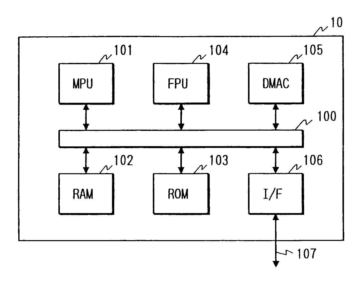
[0037]FIG. 1 illustrates the inner construction of an electronic apparatus embodying the present invention by way of example. In the embodiment shown, MPU 101, RAM 102, ROM 103, FPU (Floating-point Processing Unit) 104, DMAC (Direct Memory Access controller) 105, and interface circuit 106 are connected via bus 100 in a wiring substrate 10. What is particularly noticeable according to this embodiment is that the bus 100 does not lead out of the wiring substrate 10, but only an interface line 107 which interfaces with external devices leads out of the wiring substrate 10.

[0038]All semiconductor chips to be connected to the bus 100 are totally packaged on the wiring substrate 10 according to this embodiment. Since the bus 100 does not led out of the wiring substrate 10, the number of signal lines connecting between internal and external devices is reduced by a large margin over the prior art. Accordingly, the number of pins connecting between the signal lines inside and outside the wir...


PUM


Abstract

An electronic apparatus which includes a wiring substrate which includes wiring conductors, and a plurality of semiconductor bare chips that are formed on the wiring substrate. The semiconductor bare chips include a processor for processing data and a circuit having a checking function for detecting faults of the processor.

Description

CROSS REFERENCE TO RELATED APPLICATIONS[0001]The present application is a continuation of application Ser. No. 10 / 370,518, filed Feb. 24, 2003 now U.S. Pat. No. 6,728,904; which is a continuation of application Ser. No. 09 / 793,968, filed Feb. 28, 2001, now U.S. Pat. No. 6,584,004; which is a continuation of application Ser. No. 09 / 271,448, filed Mar. 18, 1999, now U.S. Pat. No. 6,223,273; which is a continuation of application Ser. No. 09 / 095,049, filed Jun. 10, 1998, now U.S. Pat. No. 6,195,742; which is a continuation of application Ser. No. 08 / 746,942, filed Nov. 18, 1996, now U.S. Pat. No. 5,789,805; which is a continuation of application Ser. No. 08 / 523,346, filed Sep. 5, 1995, now U.S. Pat. No. 5,614,761; which is a continuation of application Ser. No. 07 / 843,234, filed Feb. 28, 1992, now U.S. Pat. No. 5,468,992.[0002]This application is a continuation of Ser. No. 09 / 095,049, filed Jun. 10, 1998, which is a continuation of Ser. No. 08 / 746,942, filed Nov. 18, 1996, which is a c...

Claims


Application Information

Patent Timeline
Patent Type & Authority Patents(United States)
IPC IPC(8): G11C11/00G06F3/00G06F1/18G06F11/10G06F11/22G06F12/16G06F15/78G11C5/00H01L23/495H01L23/50H01L23/538H01L25/04H01L25/065H01L25/18
CPCG11C5/04G11C5/06H01L23/50H01L23/538H01L23/5386H01L24/49H01L25/0652H01L25/18H01L2224/48091H01L2224/48227H01L2224/49433H01L2224/73265H01L2924/01002H01L2924/01004H01L2924/01005H01L2924/01007H01L2924/01013H01L2924/01033H01L2924/01039H01L2924/01074H01L2924/01082H01L2924/14H01L2924/1433H01L2924/15183H01L2924/00014H01L24/48H01L2924/01019H01L2924/0102H01L2924/01055H01L2924/014H01L2924/12041H01L2924/00H01L2924/15787H01L2224/45099H01L2224/05599
Inventor KANEKAWA, NOBUYASUIHARA, HIROKAZUAKIYAMA, MASATSUGUKAWABATA, KIYOSHIYAMANAKA, HISAYOSHIOKISHIMA, TETSUYA
Owner RISING SILICON
Why Eureka
Try Eureka