Method for using data regarding manufacturing procedures integrated circuits (ICS) have undergone, such as repairs, to select procedures the ICS will undergo, such as additional repairs

Inactive Publication Date: 2006-10-10
MICRON TECH INC
View PDF122 Cites 25 Cited by
  • Summary
  • Abstract
  • Description
  • Claims
  • Application Information

AI Technical Summary

Benefits of technology

[0027]The present invention thus prevents IC's that are unrepairable from being assembled into MCM's, such as Single In-Line M

Problems solved by technology

Thus, for example, the accessed data may indicate that insufficient spare circuitry is available on an IC to effect repairs, so the IC ca

Method used


Image

  • Method for using data regarding manufacturing procedures integrated circuits (ICS) have undergone, such as repairs, to select procedures the ICS will undergo, such as additional repairs
  • Method for using data regarding manufacturing procedures integrated circuits (ICS) have undergone, such as repairs, to select procedures the ICS will undergo, such as additional repairs
  • Method for using data regarding manufacturing procedures integrated circuits (ICS) have undergone, such as repairs, to select procedures the ICS will undergo, such as additional repairs

Examples


Embodiment Construction

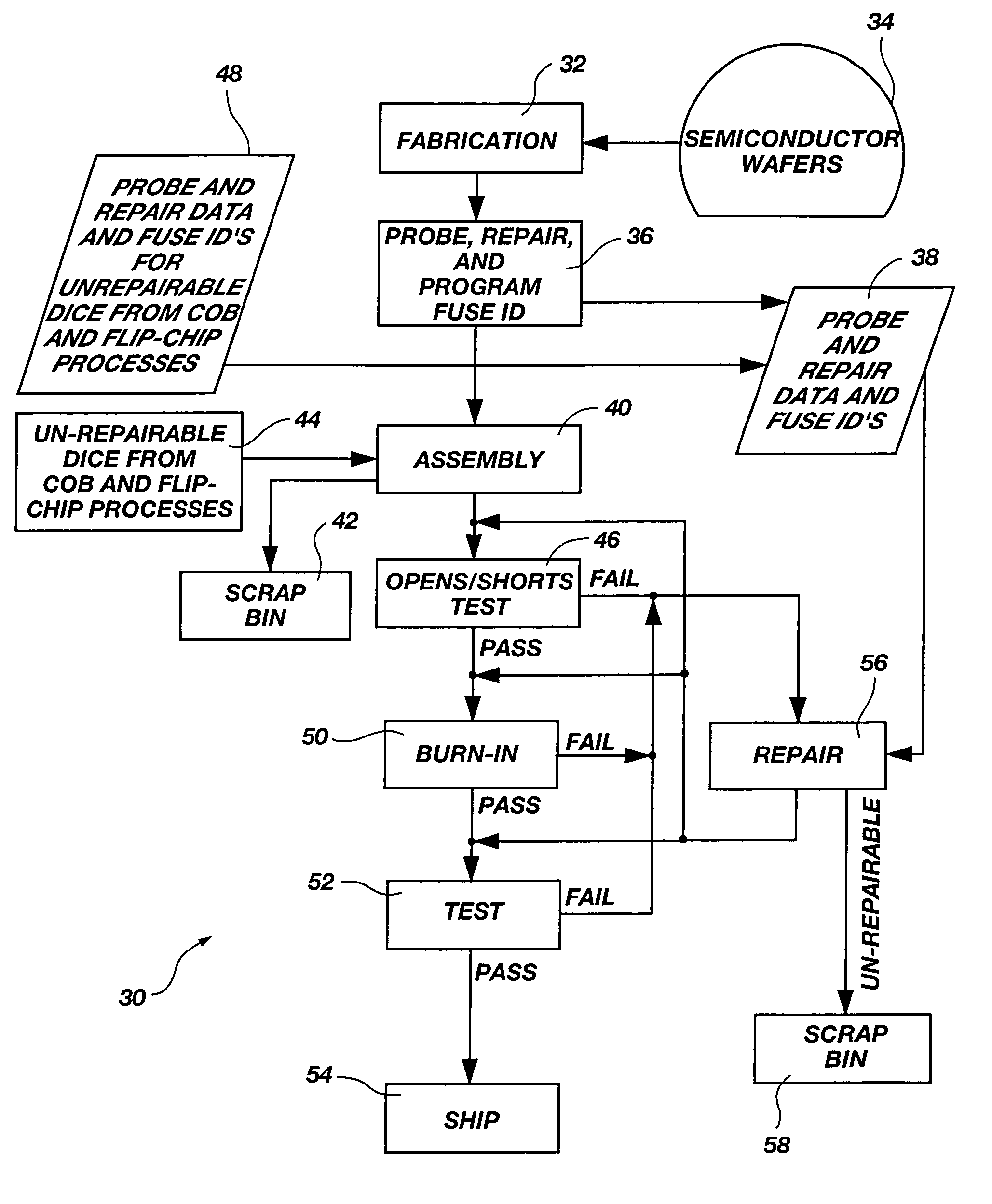
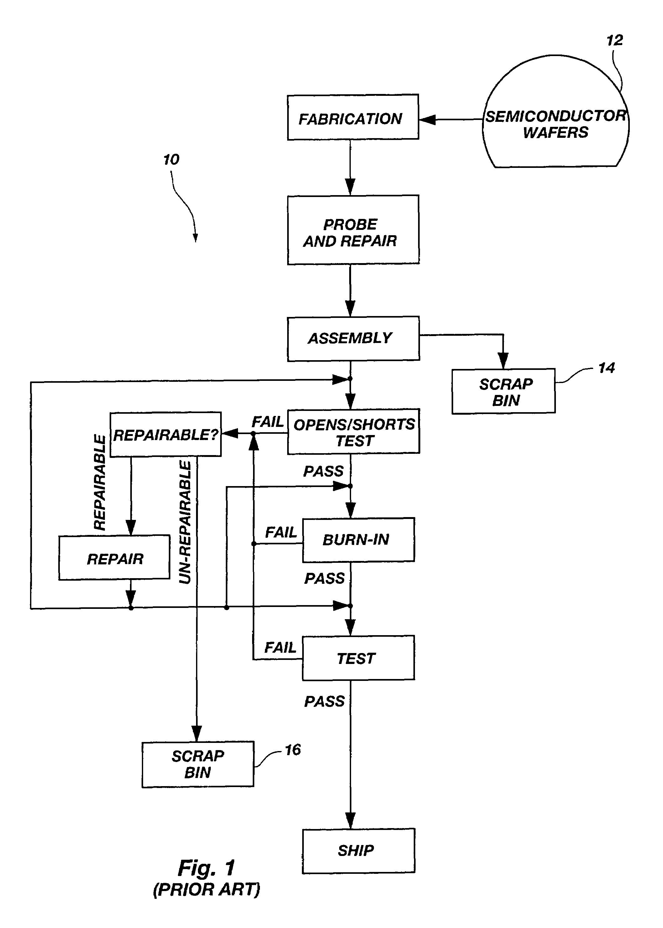
[0034]As shown in FIG. 3A, an inventive process 30 for manufacturing Dynamic Random Access Memory (DRAM) Integrated Circuit semiconductor devices (IC's) begins with DRAM IC's being fabricated in a fabrication step 32 on the surface of a semiconductor wafer 34. It will be understood by those having skill in the field of this invention that the present invention is applicable to any IC devices, including Static Random Access Memory (SRAM) IC's, Synchronous DRAM (SDRAM) IC's, processor IC's, Single In-line Memory Modules (SIMM's), Dual In-line Memory Modules (DIMM's), Rambus In-Line Memory Modules (RIMM), Small Outline Rambus In-Line Memory Modules (SO-RIMM), Personal Computer Memory Format (PCMCIA), Board-Over-Chip type substrate configurations, and other Multi-Chip Modules (MCM's). It will also be understood that although the present invention will be described below in the context of a wire bond / lead frame assembly process, either a conventional lead frame or leads-over-chip configu...


PUM


Abstract

An inventive method in an integrated circuit (IC) manufacturing process for using data regarding repair procedures conducted on IC's at probe to determine whether any further repairs will be conducted later in the manufacturing process includes storing the data in association with a fuse ID of each of the IC's. The ID codes of the IC's are automatically read, for example, at an opens/shorts test during the manufacturing process. The data stored in association with the ID codes of the IC's is then accessed, and additional repair procedures the IC's may undergo are selected in accordance with the accessed data. Thus, for example, the accessed data may indicate that an IC is unrepairable, so the IC can proceed directly to a scrap bin without having to be queried to determine whether it is repairable, as is necessary in traditional IC manufacturing processes.

Description

CROSS-REFERENCE TO RELATED APPLICATIONS[0001]This application is a continuation-in-part of application Ser. No. 09 / 292,655, filed Apr. 15, 1999, now U.S. Pat. No. 6,363,295, issued Mar. 26, 2002, which is a continuation of application Ser. No. 08 / 871,015, filed Jun. 6, 1997, now U.S. Pat. No. 5,907,492, issued May 25, 1999.[0002]This application is related to: an application having Ser. No. 08 / 591,238, filed Jan. 17, 1996, entitled “METHOD AND APPARATUS [sic] FOR STORAGE OF TEST RESULTS WITHIN AN INTEGRATED CIRCUIT”, abandoned in favor of a continuation-in-part application filed Feb. 27, 1998, having Ser. No. 09 / 032,417, and entitled “METHOD AND APPARATUS [sic] FOR STORAGE OF TEST RESULTS WITHIN AN INTEGRATED CIRCUIT”, now U.S. Pat. No. 6,194,738, issued Feb. 27, 2001; an application having Ser. No. 08 / 664,109, filed Jun. 13, 1996, entitled “A STRUCTURE AND A METHOD FOR STORING INFORMATION IN A SEMICONDUCTOR DEVICE”, now U.S. Pat. No. 5,895,962, issued Apr. 20, 1999; an application ...

Claims


Application Information

Patent Timeline
IPC IPC(8): G06F19/00G06F11/00
CPCG03F7/7065G06F11/006H01L2223/5444G16Z99/00G06F11/00
Inventor AKRAM, SALMANFARNWORTH, WARREN M.GOCHNOUR, DEREK J.HEMBREE, DAVID R.HESS, MICHAEL E.JACOBSON, JOHN O.WARK, JAMES M.WOOD, ALAN G.
Owner MICRON TECH INC
Why Eureka
Try Eureka