Method for forming a filled trench in a semiconductor layer of a semiconductor substrate, and a semiconductor substrate with a semiconductor layer having a filled trench therein

a technology of semiconductor substrate and filled trench, which is applied in the direction of semiconductor devices, electrical devices, basic electric elements, etc., can solve the problems of creating longitudinally extending voids in the trench, the surface of the silicon layer not increasing in depth at a uniform rate, and the filling of such trenches

Inactive Publication Date: 2006-10-17
ANALOG DEVICES INC
View PDF16 Cites 14 Cited by
  • Summary
  • Abstract
  • Description
  • Claims
  • Application Information

AI Technical Summary

Benefits of technology

[0013]relieving the trench adjacent the open mouth thereof for preventing the commencement of bridging of the trench with a filling material at a level adjacent the first face of the semiconductor layer as the trench is being filled, and
[0015]Preferably, the trench is sufficiently relieved for preventing commencement of bridging of the trench with the filling material at a level above a plane extending parallel to and below a plane to which the first face of the semiconductor layer is to be finished. Advantageously, the trench is relieved adjacent the open mouth thereof on one side of the trench. Ideally, the trench is relieved adjacent the open mouth thereof on respective opposite sides of the trench.
[0024]In one embodiment of the invention the trench is relieved by etching. Preferably, the etching of the trench is carried out by an RIE etch. Advantageously, the parameters of the RIE etch are controlled for minimising the depth of scallops formed by the RIE etch.
[0025]In another embodiment of the invention the forming of the trench and the relieving of the trench are carried out by the same etching process, and the parameters of the etching process are ramped during the etching process for relieving the trench. Preferably, the parameters of the etching process are controlled for minimising the formation of footings at the base of the trench.
[0048]Indeed, in certain cases by sufficiently relieving portions of the trench extending from the open mouth into the trench, the formation of voids can be entirely eliminated by the method according to the invention. By eliminating the formation of voids in a filled trench, or displacing any voids formed in the filled trench from the open mouth downwardly into the filled trench, there is no danger of voids being formed in the filled trench which could act as entrapment areas for chemicals and gases from one process step to which the semiconductor layer is subjected, which would become contaminants in a subsequent process step on leaking from the voids.

Problems solved by technology

Whether the trenches are entirely filled with a single filling material, for example, oxide or silicon nitride, or partially filled with oxide or silicon nitride and then with polysilicon, problems arise in the filling of such trenches.
Unfortunately, the depth of the layers of the filling material formed on the base and the side walls of the trench, and on the surface of the silicon layer do not increase in depth at a uniform rate.
Once the bread-loafing of the filling material has caused bridging of the trench, no further filling material can be filled into the trench, thus leading to the creation of a longitudinally extending void in the trench.
While, in general, the existence of such voids do not affect the electrical insulating characteristics of the filled trenches, they do lead to areas of entrapment where gases and liquids used in subsequent processing steps of the silicon layer can become entrapped, and subsequently lead to contamination of the silicon layer.
Such cleaning chemicals, in general, would be contaminants in subsequent processing steps of the silicon layer, and on leaking out through the voids would lead to contamination in the subsequent processing steps which is unacceptable.
Another problem arises where a photoresist layer is to be formed on the surface 6 of the silicon layer through which voids have been exposed.
The spinning of the photoresist over areas where voids are exposed leads to uneven coating in the form of streaking of the photoresist over the surface of the silicon layer.
This, thus, prevents accurate patterning of the photoresist layer.
Additionally, the photoresist may become entrapped in the voids, thus leading to contamination in subsequent processing steps.
In such cases, even where a void formed in a trench does not extend up to the open mouth of the trench, subsequent grinding of the silicon layer, can lead to the removal of the bridging of the trench, thus exposing the void.

Method used


Image

  • Method for forming a filled trench in a semiconductor layer of a semiconductor substrate, and a semiconductor substrate with a semiconductor layer having a filled trench therein
  • Method for forming a filled trench in a semiconductor layer of a semiconductor substrate, and a semiconductor substrate with a semiconductor layer having a filled trench therein
  • Method for forming a filled trench in a semiconductor layer of a semiconductor substrate, and a semiconductor substrate with a semiconductor layer having a filled trench therein

Examples


Embodiment Construction

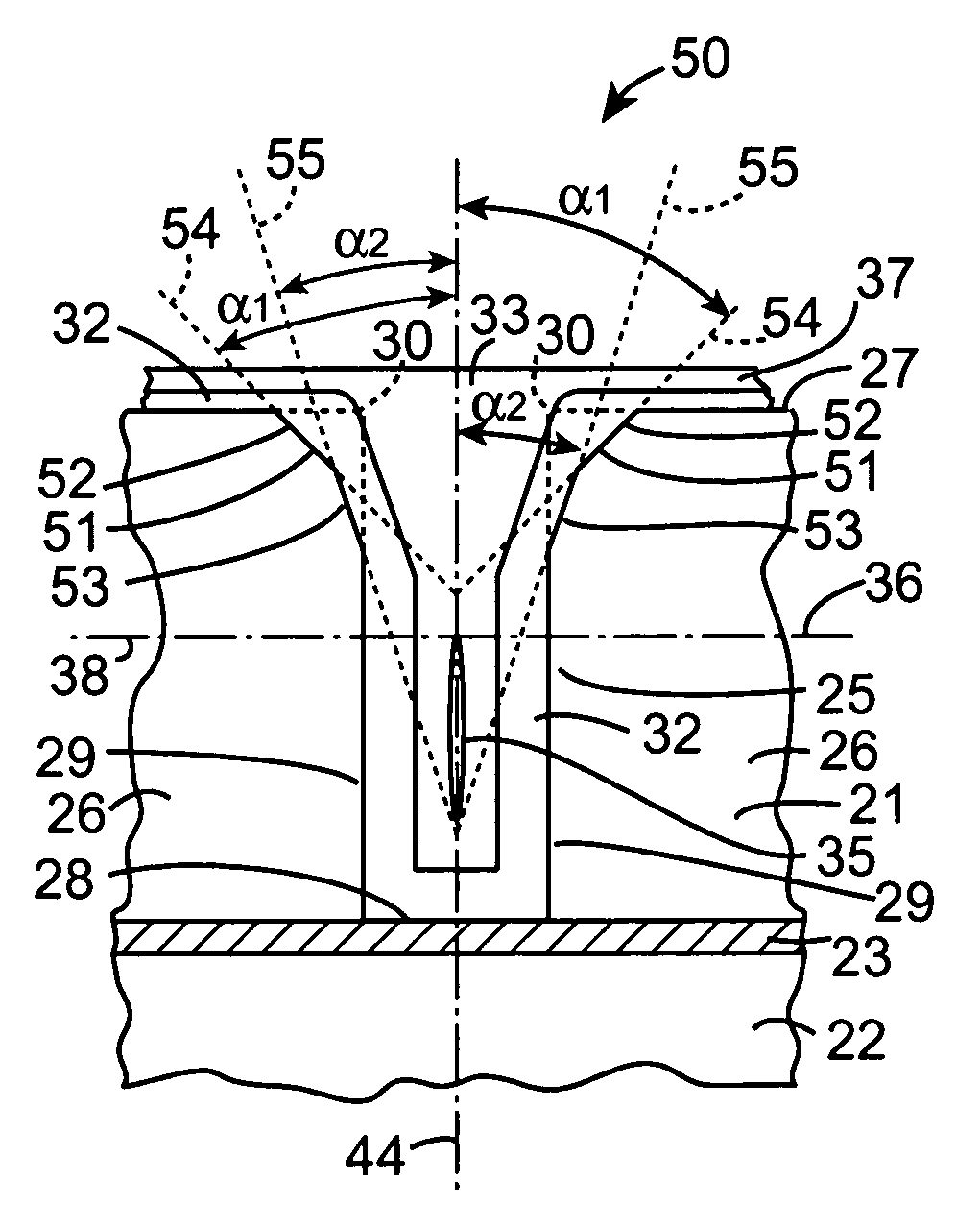
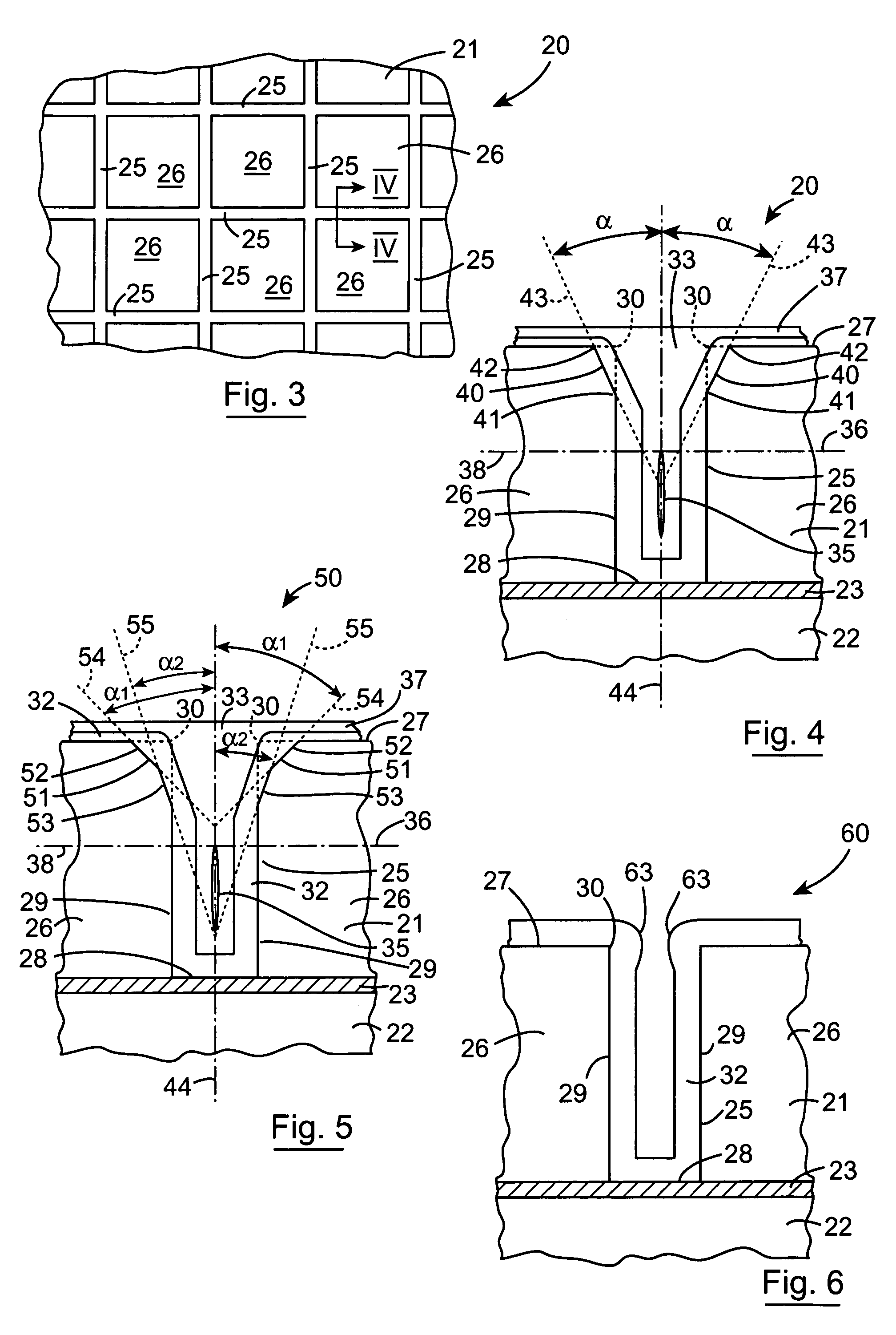
[0064]Referring now to FIGS. 3 and 4 there is illustrated a portion of an SOI structure according to the invention indicated generally by the reference numeral 20 comprising a silicon layer 21 supported on handle layer 22 with a buried insulating layer 23 located between the silicon layer 21 and the handle layer 22. The silicon layer 21 and the handle layer 22 are formed from respective silicon wafers of single crystal silicon, and the buried insulating layer 23 is an oxide layer which may be thermally grown or deposited on either the handle layer 22 or the silicon layer 21 and then bonded to the other of the two layers. Alternatively, the oxide layer 23 may be thermally grown or deposited on both the silicon layer 21 and the handle layer 22, and then both oxide layers can be bonded together. The construction of such SOI structures will be well known to those skilled in the art. Filled electrical isolating trenches 25 are formed by a method according to the invention in the silicon ...


PUM


Abstract

A method for forming an isolation filled trench (25) in a silicon layer (21) of an SOI structure (20). The trench (25) is relieved adjacent its open mouth (30) in order to displace the commencement of bridging of the trench (25) with the filling material, to a level (36) well below a first surface (27) of the silicon layer (21) for in turn displacing voids (35) from the open mouth (30) into the trench (25) below the level (36). The trench may be relieved by forming tapered portions (40) in the side wells (29) adjacent the open mouth (30), and / or by relieving one or more lining layers (32) in the trench (25) adjacent the open mouth (30) to form tapered portion (52) and (53). Instead of relieving the trench (25) by tapering the side walls (29) relieving recesses may be formed into the first surface (27) of the silicon layer (21) adjacent the open mouth (30). By relieving the trench (25) or one or more of the lining layers (32) adjacent the open mouth (30) the commencement of bridging of the trench with the filling material is displaced downwardly to a level (36), which displaces voids formed in the trench below the level (36). By sufficiently relieving the trench (25) and / or lining layers (32) adjacent the open mouth to a sufficient depth the formation of voids in the trench may be completely avoided.

Description

FIELD OF THE INVENTION[0001]The present invention relates to a method for forming a filled trench in a semiconductor layer of a semiconductor substrate, and in particular, to such a method for forming a filled trench with the effect of trench voids minimised. The invention also relates to a semiconductor substrate with a semiconductor layer having a filled trench formed therein with the effect of trench voids minimised.BACKGROUND TO THE INVENTION[0002]A trench isolated silicon layer in a semiconductor substrate is commonly required. For example, where it is desired to electrically insulate discrete areas of a silicon layer one from the other trenches filled with electrically insulating filling material are formed in the silicon layer for electrically insulating the respective discrete areas. Commonly, such layers requiring trench filled isolation may be a silicon layer of a silicon on insulator (SOI) structure. A buried insulating layer, typically, an oxide layer is located under th...

Claims


Application Information

Patent Timeline
Patent Type & Authority Patents(United States)
IPC IPC(8): H01L21/8238H01L29/00H01L21/762H01L21/763H01L21/768
CPCH01L21/76232H01L21/76283H01L21/76286
Inventor NEVIN, WILLIAM ANDREWGORMLEY, COLIN STEPHEN
Owner ANALOG DEVICES INC
Why Eureka
Try Eureka