Semiconductor integrated circuit

a technology of integrated circuits and semiconductors, applied in the direction of power consumption reduction, pulse techniques, instruments, etc., can solve the problems of large volume of leakage current flow of transistors, large amount of electricity consumed, interference with the accelerated operation, etc., and achieve the effect of reducing power consumption, reducing wiring length, and reducing wiring length

Active Publication Date: 2006-10-17
SOCIONEXT INC
View PDF8 Cites 33 Cited by
  • Summary
  • Abstract
  • Description
  • Claims
  • Application Information

AI Technical Summary

Benefits of technology

[0011]According to the foregoing configuration, the control potential of the MOS transistor (at least one of substrate potential and source potential) is controlled to there by control an absolute value of a threshold voltage of the MOS transistor. When the control potential is controlled in such manner that the absolute value of the threshold voltage becomes larger, a leakage current flowing when the MOS transistor is turned off can be reduced. Further, resistance to a glitch noise due to an influence from crosstalk can be increased, and when the control potential is controlled in such manner as to obtain the small absolute value of the threshold voltage, an operation can be accelerated.
[0039]When the semiconductor integrated circuit is divided into a plurality of areas and a plurality of MOS transistors included in one of the areas logically operate in a same manner, it is preferable for the plurality of transistors operating in the same manner to be collectively controlled by a substrate potential control circuit or a source potential control circuit. In the case of being connected to other than the clock tree, the wiring length can be shortened, and the substrate potential or source potential can be thereby effectively controlled.

Problems solved by technology

A large-scale semiconductor integrated circuit in recent years enjoys a higher operation speed resulting from a higher integration thereof, while consuming a larger amount of electricity.
However, the reduction of the power-supply voltage leads to a reduction of a current flow required for operating an MOS transistor, which interferes with the accelerated operation.
A method for avoiding the inconvenience is to reduce an absolute value of a threshold voltage of the transistor in compliance with the reduction of the power-supply voltage, however the reduction of the absolute value of the threshold voltage results in a large volume of a leakage current flow of the transistor.
In such a situation, it is impossible to satisfactorily control the leakage current flow.

Method used


Image

  • Semiconductor integrated circuit
  • Semiconductor integrated circuit
  • Semiconductor integrated circuit

Examples


Embodiment Construction

[0054]Hereinafter, embodiments of a semiconductor integrated circuit according to the present invention are described referring to the drawings.

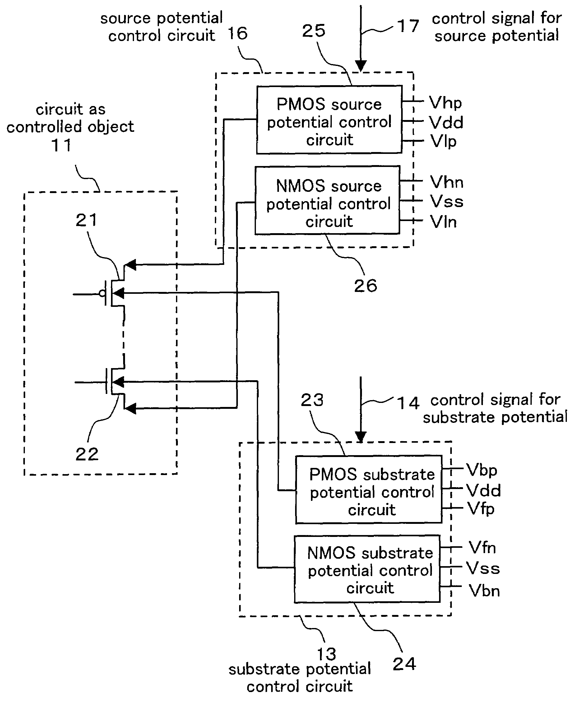
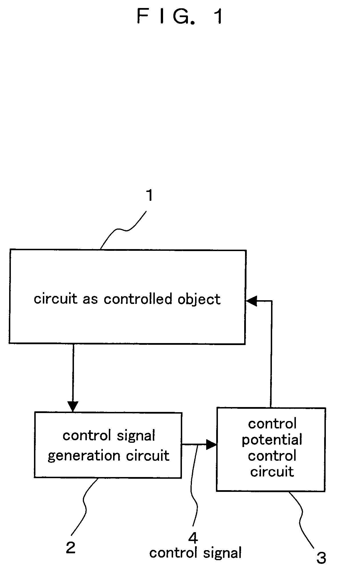
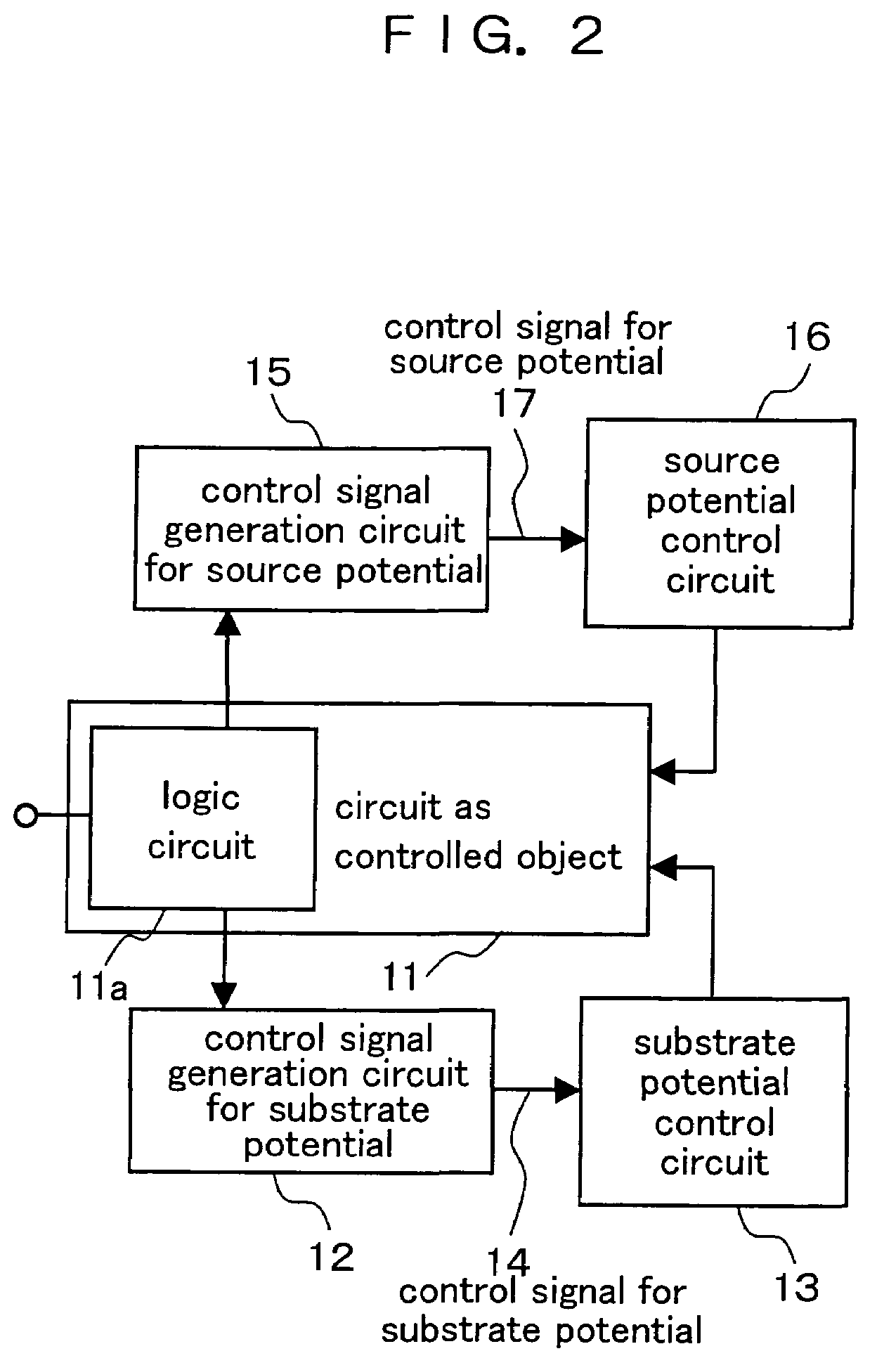
[0055]First, a basic embodiment of the present invention is described referring to FIG. 1. In FIG. 1, a reference numeral 1 denotes a circuit as a controlled object including a plurality of MOS transistors, wherein a control potential of at least one MOS transistor of the plurality of MOS transistors (at least one of substrate potential and source potential) is to be controlled. A reference numeral 2 denotes a control signal generation circuit. A reference numeral 3 denotes a control potential control circuit, and a reference numeral 4 denotes a control signal.

[0056]The circuit as the controlled object is comprised of a plurality of logic elements such as a flip-flop, inverter, AND circuit, in which a signal is propagated to thereby realize a certain logic. Therefore, the circuit as the controlled object differs to such a memory cell array a...


PUM


Abstract

A semiconductor integrated circuit according to the present invention comprises a circuit as a controlled object including an MOS transistor, wherein a control potential (at least one of a substrate potential and source potential) is to be controlled, a control signal generation circuit for generating a control signal with respect to the control potential based on an internal signal of the circuit as the controlled object, and a control potential control circuit for controlling the control potential (substrate potential / source potential) of the MOS transistor based on the control signal.

Description

BACKGROUND OF THE INVENTION[0001]1. Field of the Invention[0002]The present invention relates to a semiconductor integrated circuit including an MOS transistor, in particular to a technology for realizing a higher speed and reduced power consumption by controlling a control potential (substrate potential or source potential) of the MOS transistor.[0003]2. Description of the Related Art[0004]A large-scale semiconductor integrated circuit in recent years enjoys a higher operation speed resulting from a higher integration thereof, while consuming a larger amount of electricity. When a power-supply voltage is reduced, power consumption can be accordingly reduced. However, the reduction of the power-supply voltage leads to a reduction of a current flow required for operating an MOS transistor, which interferes with the accelerated operation. A method for avoiding the inconvenience is to reduce an absolute value of a threshold voltage of the transistor in compliance with the reduction of ...

Claims


Application Information

Patent Timeline
Patent Type & Authority Patents(United States)
IPC IPC(8): G05F1/10G11C5/14H01L21/822G11C7/00H01L21/8234H01L27/04H01L27/088H03K19/00H03K19/01H03K19/094H03K19/0948
CPCH03K19/0016H03K19/0013H03K19/017
Inventor HATAKEYAMA, KAORISUMITA, MASAYAKISHISHITA, KEISUKENUMA, MICHIO
Owner SOCIONEXT INC
Why Eureka
Try Eureka