Semiconductor integrated circuit device having static random access memory mounted thereon

a technology of integrated circuit devices and static random access memory, which is applied in static storage, digital storage, instruments, etc., can solve the problems of increasing memory capacity and a lowering of voltage, data destruction due to power supply voltage noise in the chip becoming more difficult to occur, and narrowing

Inactive Publication Date: 2006-10-17
KK TOSHIBA
View PDF6 Cites 38 Cited by
  • Summary
  • Abstract
  • Description
  • Claims
  • Application Information

AI Technical Summary

Problems solved by technology

In recent years, various problems appear in the SRAM with an increase in the memory capacity and a lowering in the voltage.
Generally, the stability of data stored in the SRAM cell becomes higher and data destruction due to power supply voltage noise in the chip becomes more difficult to occur as the static noise margin becomes larger.
In recent years, as the SRAM cell is miniaturized and the driving voltage becomes lower, the problems that the set window of the threshold voltage of the driver transistor which simultaneously satisfies the above two conditions becomes narrower and the cell designing becomes difficult occur.

Method used


Image

  • Semiconductor integrated circuit device having static random access memory mounted thereon
  • Semiconductor integrated circuit device having static random access memory mounted thereon
  • Semiconductor integrated circuit device having static random access memory mounted thereon

Examples


first embodiment

[0032

[0033]First, a semiconductor integrated circuit device having a static random access memory of a first embodiment of the present invention is explained with reference to FIGS. 3 to 10.

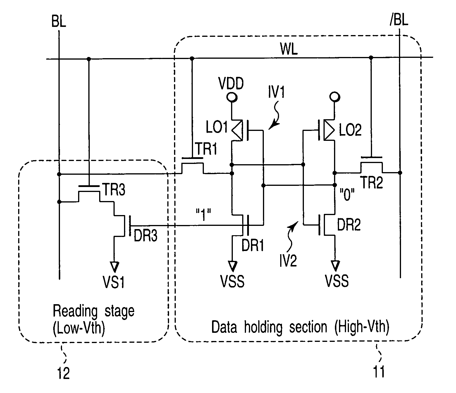
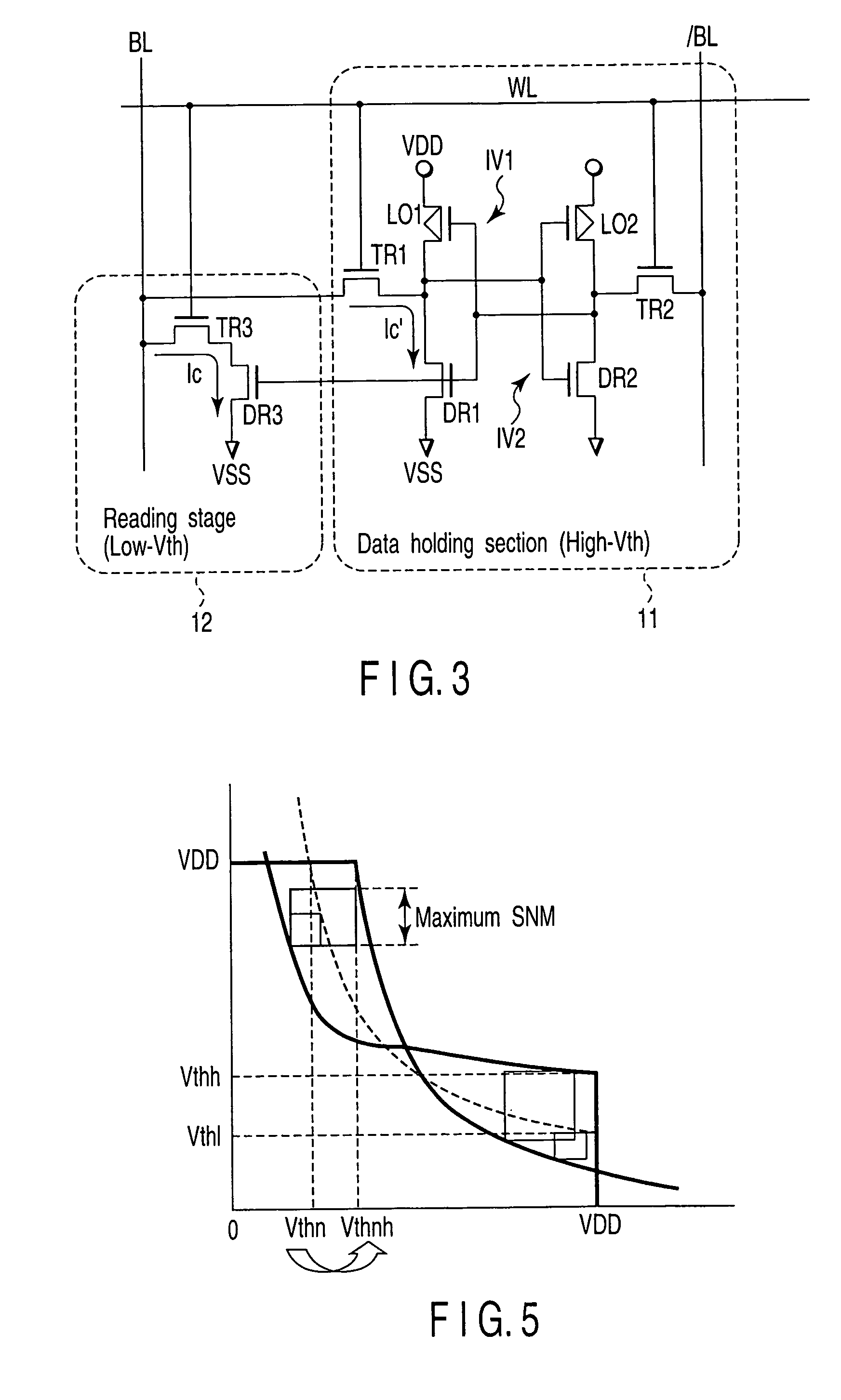
[0034]FIG. 3 is a circuit diagram showing the configuration of an SRAM cell according to the first embodiment. The SRAM cell includes a data holding section 11 configured by six transistors and a reading stage 12 configured by two N-channel MOS field effect transistors (which are hereinafter referred to as NMOS transistors). The data holding section 11 includes a first inverter IV1, second inverter IV2, first transfer gate transistor TR1 and second transfer gate transistor TR2. The reading stage 12 includes a third transfer gate transistor TR3 and read driver transistor DR3. The first inverter IV1 includes a first load transistor LO1 and first driver transistor DR1 and the second inverter IV2 includes a second load transistor LO2 and second driver transistor DR2.

[0035]The first, second load transi...

second embodiment

[0067

[0068]Next, a semiconductor integrated circuit device containing an SRAM according to a second embodiment of the present invention is explained. The same reference symbols are attached to the same portions as those in the configuration of the first embodiment.

[0069]FIG. 11 is a circuit diagram showing the configuration of an SRAM according to the second embodiment of the present invention. In the first embodiment shown in FIG. 3, voltage supplied to the source terminal of the read driver transistor DR3 is fixed at the reference voltage such as the ground potential. On the other hand, in the second embodiment, voltage VS1 supplied to the source terminal of the read driver transistor DR3 is not fixed at the reference voltage such as the ground potential. Further, the voltage is selectively set at the ground potential or voltage such as the power supply voltage VDD higher than the ground potential. The other configuration is the same as that of the first embodiment.

[0070]The sourc...

third embodiment

[0071

[0072]Next, a semiconductor integrated circuit device containing an SRAM according to a third embodiment of the present invention is explained. The same reference symbols are attached to the same portions as those in the configuration of the first embodiment.

[0073]FIG. 12 is a circuit diagram of an SRAM cell according to the third embodiment of the present invention. The SRAM cell of the first and second embodiments is an 8-transistor type cell based on the one-side bit line read system, but the SRAM cell of the third embodiment is a 10-transistor type cell based on the both-side bit line read system. A reading stage 13 is also provided on the bit line / BL side to configure an SRAM cell configured by ten transistors. The reading stage 13 additionally includes a fourth transfer gate transistor TR4 and read driver transistor DR4. The cell area of the SRAM cell is increased by 40% in comparison with that of the conventional 6-transistor type SRAM cell, but the read operation of hi...


PUM


Abstract

A semiconductor integrated circuit device is configured by eight transistors including the six transistors configuring the data holding section and the two NMOS transistors configuring the reading stage. The threshold voltage of the NMOS transistors configuring the reading stage is set low and the threshold voltage of the six transistors configuring the data holding section is set higher than the threshold voltage of the NMOS transistors configuring the reading stage. The cell current flowing from the bit line to the ground terminal can be set large and the large static noise margin (SNM) can be attained.

Description

CROSS-REFERENCE TO RELATED APPLICATIONS[0001]This application is based upon and claims the benefit of priority from prior Japanese Patent Application No. 2004-120265, filed Apr. 15, 2004, the entire contents of which are incorporated herein by reference.BACKGROUND OF THE INVENTION[0002]1. Field of the Invention[0003]This invention relates to a static random access memory (which is hereinafter referred to as an SRAM) and is utilized for a semiconductor integrated circuit device having an SRAM mounted thereon, for example.[0004]2. Description of the Related Art[0005]In recent years, various problems appear in the SRAM with an increase in the memory capacity and a lowering in the voltage. The prior art of the SRAM and the problem associated therewith are explained below with reference to FIGS. 1 and 2.[0006]FIG. 1 is a circuit diagram of a memory cell (which is hereinafter referred to as an SRAM cell) used to configure a conventional 6-transistor SRAM. The conventional SRAM cell has fi...

Claims


Application Information

Patent Timeline
Patent Type & Authority Patents(United States)
IPC IPC(8): G11C11/00G11C11/41G11C11/412
CPCG11C11/412Y10S257/903Y10S257/904
Inventor YABE, TOMOAKI
Owner KK TOSHIBA
Why Eureka
Try Eureka