Integrated proof flow system and method

a proof flow and integrated technology, applied in the field of functional verification of properties, can solve the problems of expensive re-spin of designs, re-manufacturing of chips that can be very time-consuming, and the most time-consuming component of verification

Inactive Publication Date: 2006-10-17
CADENCE DESIGN SYST INC
View PDF8 Cites 18 Cited by
  • Summary
  • Abstract
  • Description
  • Claims
  • Application Information

AI Technical Summary

Benefits of technology

[0012]Some embodiments of the present invention provide proof flow methods that integrate formal verification and nonformal verificati

Problems solved by technology

Verification is typically the most time-consuming component in a circuit design process.
Failing to detect functional design errors early in the design stages usually leads to expensive re-spin of the designs.
This re-spin includes diagnosis and correction of the errors, logic and physical re-synthesis, and even re-manufacturing of the chips that can be very time-consuming, costly and delay the time-to-market of a product.
If the chip designs are already used in some released products, this can even lead to product recalls that are very devastating to a company.
However, due to the exceedingly large and complex circuits that are being designed today, formal verification is subject to the classical state explosion problem.
The number of possible value combinations (or states) that are required to be checked by formal verification techniques is extremely large, and some states can only be reached after a very large number of cycles.
It is therefore very difficult to perform state space search exhaustively for large designs.
Such

Method used


Image

  • Integrated proof flow system and method
  • Integrated proof flow system and method
  • Integrated proof flow system and method

Examples


Embodiment Construction

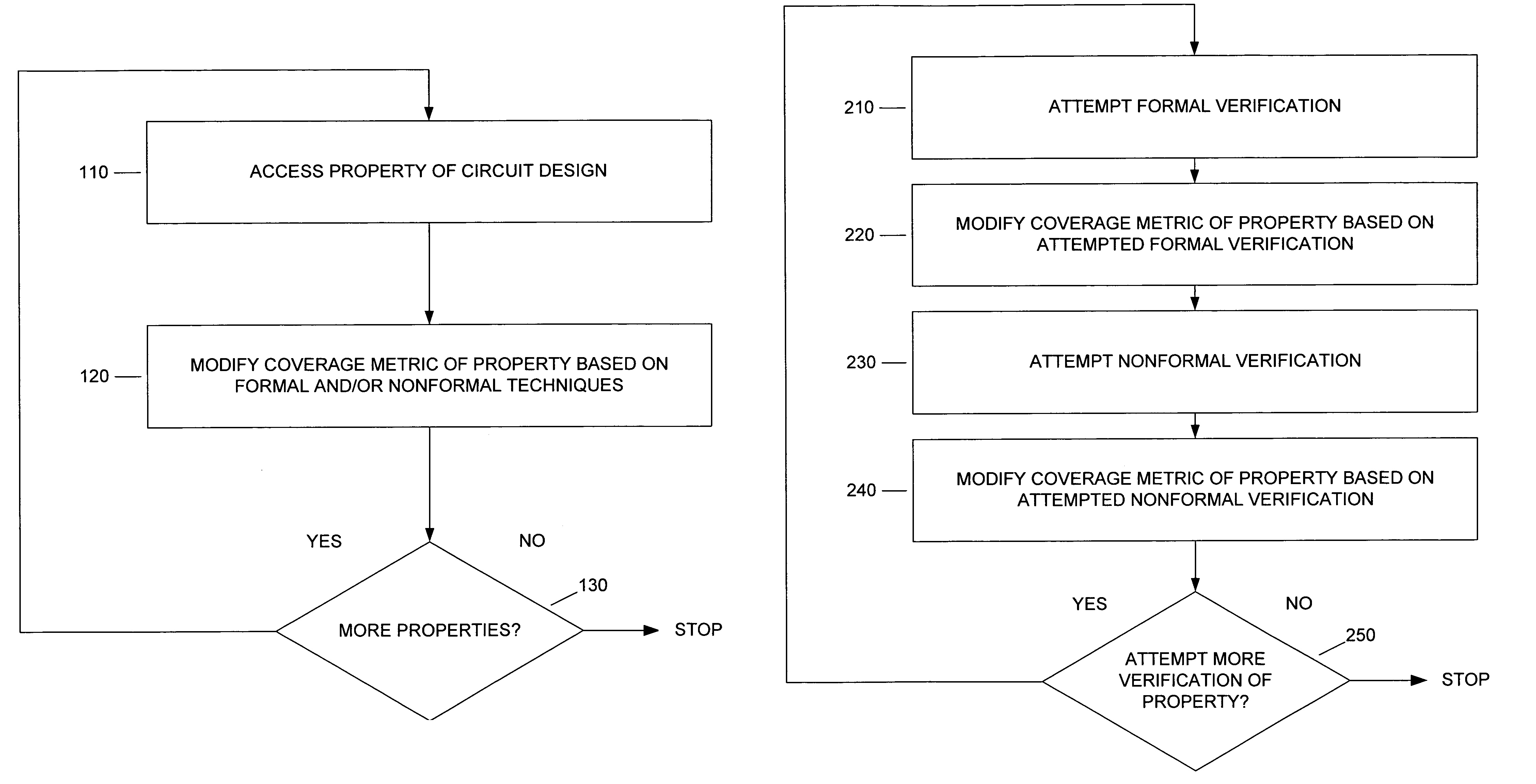
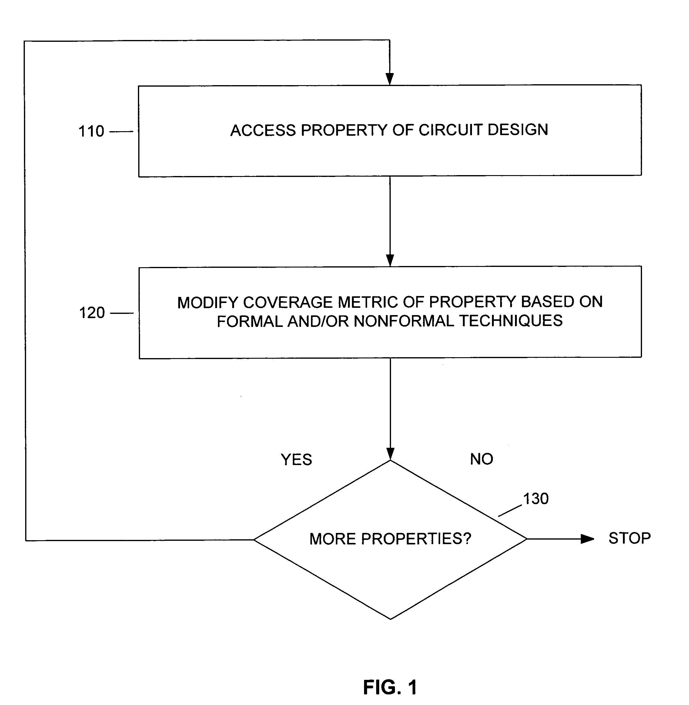
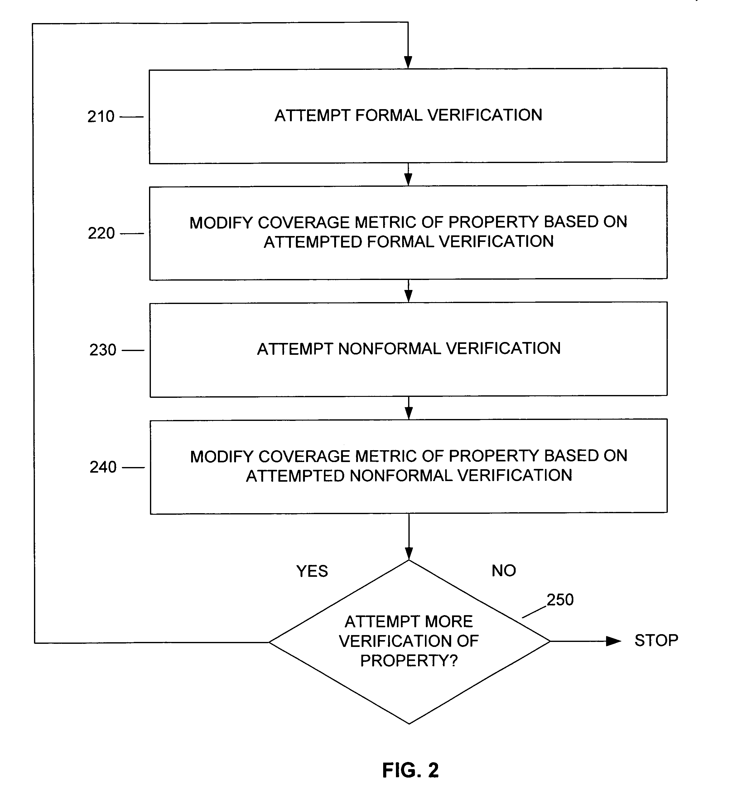
[0017]Referring to FIG. 1, one embodiment of a proof flow method for a set of properties associated with a circuit design is illustrated. Examples of properties are “signal A should always be True” and “signals A, B, and C should always satisfy the relationship that A×B=C for all clock “cycles”.

[0018]For a given property, one or more coverage metrics can be defined. If multiple coverage metrics are defined for a given property, the multiple coverage metrics can be of the same or different kinds. In the case where at least two coverage metrics of the same kind exist, different criteria can be used (e.g., if at least two metrics are of the toggle-based metric type, the sequential elements can have different weights when calculating the overall coverage).

[0019]One such metric is the state-based metric, where the goal is to search all the reachable states of the circuit and check the correctness of the property in each of the states. If the property can be verified by formal verificatio...


PUM


Abstract

Integrated proof flow methods and apparatuses are discussed. Integrated proof flow refers to attempting both formal verification and nonformal verification. A coverage metric can be changed by both attempting formal verification and by attempting nonformal verification. Some embodiments of the present invention provide proof flow methods that integrate verification and nonformal verification (e.g., bounded verification, multi-point proof, and/or vector-based simulation) to prove one or more properties in a circuit design.

Description

BACKGROUND OF THE INVENTION[0001]The present invention relates generally to functional verification of properties associated with circuit designs and, more particularly, to an integrated proof flow for the verification of such properties.DESCRIPTION OF THE RELATED ART[0002]Verification is typically the most time-consuming component in a circuit design process. Failing to detect functional design errors early in the design stages usually leads to expensive re-spin of the designs. This re-spin includes diagnosis and correction of the errors, logic and physical re-synthesis, and even re-manufacturing of the chips that can be very time-consuming, costly and delay the time-to-market of a product. If the chip designs are already used in some released products, this can even lead to product recalls that are very devastating to a company.[0003]Property checking is an approach for verifying the functionality of a circuit design. It involves proving one or more properties specified for a circ...

Claims


Application Information

Patent Timeline
IPC IPC(8): G06F17/50
CPCG06F17/504G06F30/3323
Inventor CHEN, KUANG-CHIENWANG, BOW-YAW
Owner CADENCE DESIGN SYST INC
Why Eureka
Try Eureka