Integrated circuits with contemporaneously formed array electrodes and logic interconnects

a logic interconnection and integrated circuit technology, applied in the direction of digital storage, semiconductor/solid-state device details, digital storage, etc., can solve the problems of low processing efficiency, low processing efficiency, and low processing efficiency of conventional non-volatile memory, so as to save processing steps and time, fewer processing steps, and less time

Inactive Publication Date: 2006-10-24
MICRON TECH INC
View PDF25 Cites 13 Cited by
  • Summary
  • Abstract
  • Description
  • Claims
  • Application Information

AI Technical Summary

Benefits of technology

[0010]Embodiments of the invention include a fabrication process and an apparatus for providing interconnects in a memory device. Advantageously, embodiments of the invention contemporaneously form electrodes for memory arrays and interconnects for logic circuits at the same time. This advantageously saves processing steps and time as compared to forming electrodes and forming interconnects in separate steps. With fewer processing steps, integrated circuits can be formed in less time and with fewer sources of error.
[0011]One embodiment of the invention is an integrated circuit memory device. The integrated circuit device has a semiconductor substrate assembly. Memory cell storage devices, such as MRAM memory cell storage devices are arranged in a memory array above the substrate assembly. A plurality of metallization layers form electrodes for the memory array. At least one of these metallization layers is also configured to form interconnects for logic circuits. In one embodiment, an optional cladding of a magnetic material, such as nickel-iron, forms a magnetic keepe for the electrodes. in one embodiment, the electrodes for the memory array and the interconnects for the logic circuits have unequal pitches. This can advantageously reduce electromigration, reduce distributed capacitance, etc.
[0012]Another embodiment of the invention is a method of forming electrodes and interconnects for an integrated circuit memory device. A metallization layer is formed. Electrodes for a memory array and interconnects for logic are simultaneously formed from the metallization layer. This advantageously saves processes steps, thereby speeding up manufacturing processes and decreasing the number of process steps to fabricate electrodes and / or interconnects.

Problems solved by technology

A volatile memory loses its data when power is removed.
In addition, certain volatile memories such as DRAM devices require periodic refresh cycles to retain data even when power is continuously supplied.
Disadvantageously, conventional nonvolatile memories are relatively large (physically), slow, and expensive.
Further, conventional nonvolatile memories are relatively limited in write cycle capability and typically can only be programmed to store data about 10,000 times in a particular memory location.
The fabrication of multiple layers of metallization can be time consuming and expensive.

Method used


Image

  • Integrated circuits with contemporaneously formed array electrodes and logic interconnects
  • Integrated circuits with contemporaneously formed array electrodes and logic interconnects
  • Integrated circuits with contemporaneously formed array electrodes and logic interconnects

Examples


Embodiment Construction

[0017]Although this invention will be described in terms of certain preferred embodiments, other embodiments that are apparent to those of ordinary skill in the art, including embodiments that do not provide all of the benefits and features set forth herein, are also within the scope of this invention. Accordingly, the scope of the invention is defined only by reference to the appended claims.

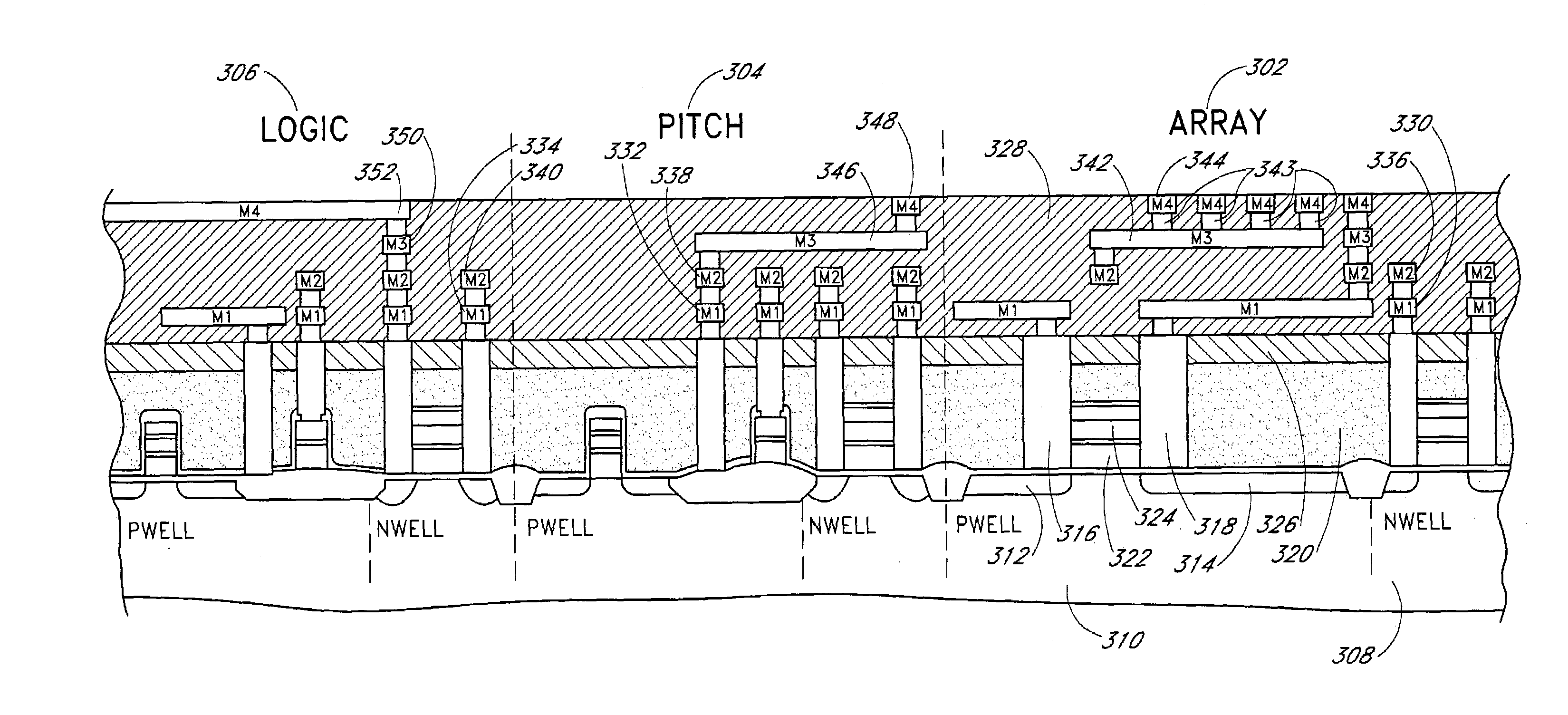
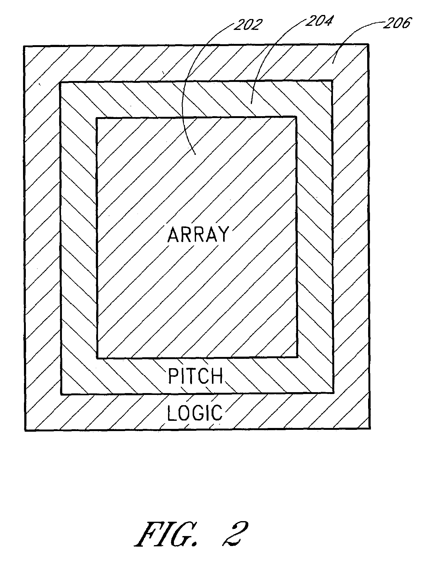
[0018]The invention relates to metallization for an integrated circuit, including an integrated circuit memory device. Embodiments of the invention include processes to fabricate interconnects for memory devices in relatively few steps. Embodiments of the invention also include memory devices with metallization layers having unequal pitch dimensions in different areas of the chip, thereby permitting simultaneous fabrication of array electrodes and logic interconnects in different areas of the chip. This reduces the number of fabrication steps used to make interconnects, thereby reducing sources...


PUM


Abstract

The invention relates to interconnects for an integrated circuit memory device. Embodiments of the invention include processes to fabricate interconnects for memory devices in relatively few steps. Embodiments of the invention further include memory devices with metallization layers having unequal pitch dimensions in different areas of the chip, thereby permitting simultaneous fabrication of array electrodes and electrical interconnects in different areas of the chip. This reduces the number of fabrication steps used to make interconnects, thereby speeding up fabrication and reducing production costs.

Description

BACKGROUND OF THE INVENTION[0001]1. Field of the Invention[0002]The invention generally relates to methods and apparatus for metallization in data storage devices for integrated circuits, and more particularly, to randomly accessible memory devices.[0003]2. Description of the Related Art[0004]Computers and other digital systems use memory to store programs and data. A common form of memory is random access memory (RAM). Many memory devices, such as dynamic random access memory (DRAM) devices and static random access memory (SRAM) devices are volatile memories. A volatile memory loses its data when power is removed. For example, after a conventional personal computer is powered off, the volatile memory is typically reloaded through a boot up process upon a restart. In addition, certain volatile memories such as DRAM devices require periodic refresh cycles to retain data even when power is continuously supplied.[0005]Nonvolatile memory devices retain data for long periods of time when...

Claims


Application Information

Patent Timeline
Patent Type & Authority Patents(United States)
IPC IPC(8): H01L23/48G11C5/06G11C11/14H01L21/8242H01L27/105H01L27/108H01L27/22
CPCG11C5/06G11C11/14H01L27/105H01L27/10882H01L27/10897H01L27/228H10B61/22H10B12/48H10B12/50
Inventor SEYYEDY, MIRMAJIDHUSH, GLEN E.TUTTLE, MARK E.VOLLMAN, TERRY C.
Owner MICRON TECH INC
Why Eureka
Try Eureka