Optical scanning device

a scanning device and optical technology, applied in the field of optical scanning devices, can solve the problems of increasing the cost of scanning devices' manufacture, wasting certain amounts of input light, and deteriorating the resolution of optical spots formed, so as to reduce astigmatism and less radiation energy loss

Inactive Publication Date: 2006-10-24
KONINKLIJKE PHILIPS ELECTRONICS NV
View PDF7 Cites 4 Cited by
  • Summary
  • Abstract
  • Description
  • Claims
  • Application Information

AI Technical Summary

Benefits of technology

[0015]The second surface preferably has a pattern of stepped annular zones which is non-periodic, i.e., one which does not regularly repeat in the radial direction, and, therefore, does not form diffraction orders. As a consequence, the phase structure does not have the inherent losses of a grating. The optical element introduces the required wavefront changes with less loss of radiation energy. Arranging the step-like structure with plane-parallel reflective surfaces, has an advantage in that astigmatism can be reduced.

Problems solved by technology

Without compensating measures, refocusing from one layer to the other results in spherical aberration, generating a wavefront error of 200–300 mλ root mean square optical path difference (OPD (rms)), which deteriorates the resolution of the optical spot formed.
However, using mechanical actuators to provide spherical aberration compensation, particularly when a separate mechanical actuator is used to provide focus control, is relatively complex and, therefore, increases the cost of manufacture of the scanning device.
Due to the diffraction, a certain amount of the input light is wasted, which is undesirable.

Method used


Image

  • Optical scanning device
  • Optical scanning device
  • Optical scanning device

Examples


Embodiment Construction

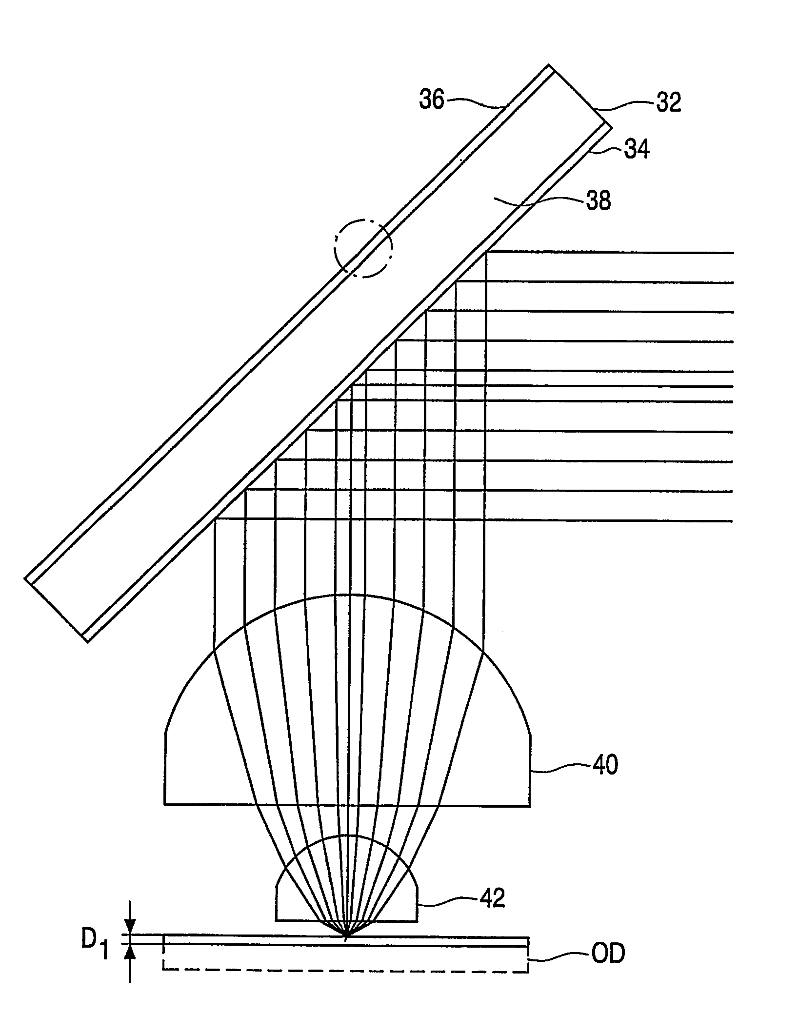
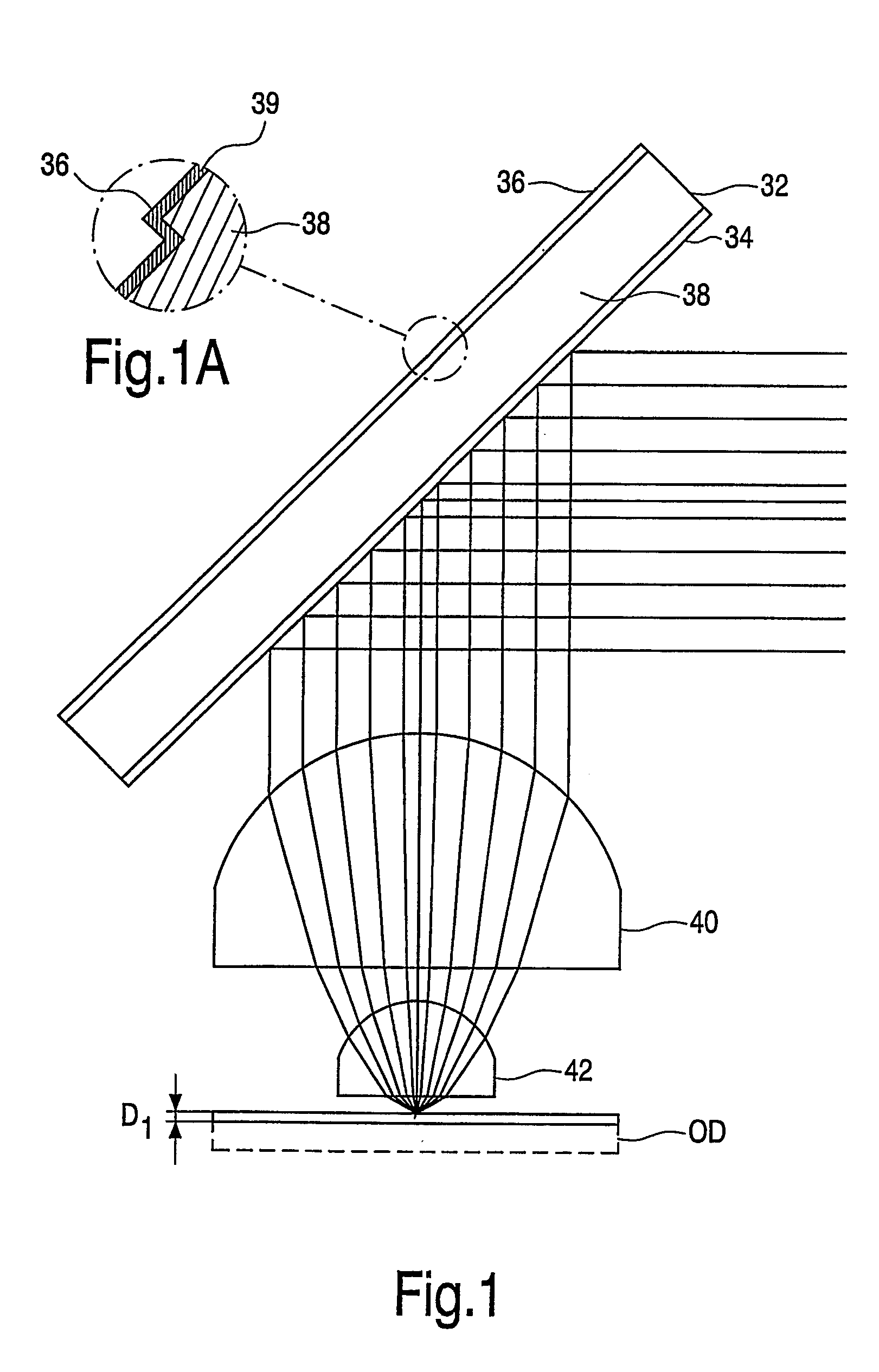
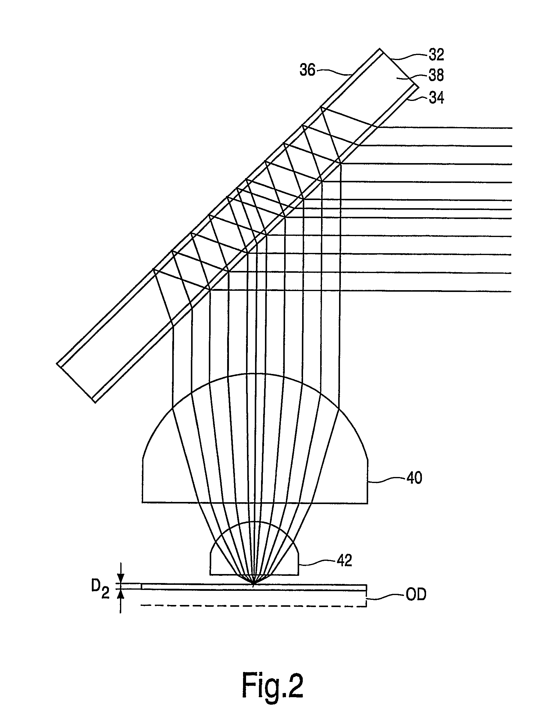
[0023]FIG. 1 illustrates a phase modifying folding mirror 32 arranged in an optical scanning device in accordance with one embodiment of the invention. The folding mirror 32 includes a first reflective surface 34 formed from a thin-film laminar structure, similar to that used in polarizing beam splitters, having polarizing characteristics. The first surface 34 reflects radiation impinging upon it at a 45° angle with a first polarization, and transmits radiation impinging upon it from the same angle with a second, orthogonal polarization.

[0024]A second reflective surface 36 is arranged to the opposite side of the folding mirror 32. As shown in FIG. 1A, the second reflective surface is coated in a mirroring material, for example, a thin metallic film, 39, and the surface 36 includes a non-planar phase structure in the form of stepped annular zones, the zones forming a non-periodic pattern of different heights corresponding to a wavefront aberration to be generated when radiation of th...


PUM

PropertyMeasurementUnit
angleaaaaaaaaaa
optical path differenceaaaaaaaaaa
thicknessaaaaaaaaaa

Abstract

An optical scanning device for scanning a dual-layer optical record carrier. The device includes a spherical aberration compensation optical subsystem having a switchable liquid crystal cell (10) for altering a wavefront deviation generated in a folding mirror (32) including a non-periodic phase structure (NPS) located behind a polarization-selective reflective layer.

Description

BACKGROUND OF THE INVENTION[0001]1. Field of the Invention[0002]This invention relates to an optical scanning device, and an optical element for use therein, for scanning an optical record carrier, such as an optical disk, comprising an information layer, the device comprising a radiation source for generating a radiation beam and an objective lens, located in an optical path between the radiation source and the information layer, for converging the radiation beam to a spot on the information layer. In particular, but not exclusively, the invention relates to an optical scanning device including an optical element to compensate for spherical aberrations generated by different optical path lengths (referred to herein as information layer depths) through which the beam travels in an optical disk to reach an information layer in the disk.[0003]2. Description of the Related Art[0004]There is a need for the production of optical record carriers of high capacity. Therefore, optical scanni...

Claims


Application Information

Patent Timeline
Patent Type & Authority Patents(United States)
IPC IPC(8): G11B7/00G02B5/00G02B5/30G11B7/135
CPCG11B7/1362G11B7/1367G11B7/1369G11B7/13925G11B2007/0013G11B7/1365G02B5/30
Inventor HENDRIKS, BERNARDUS HENDRIKUS WILHELMUSDE VRIES, JORRIT ERNST
Owner KONINKLIJKE PHILIPS ELECTRONICS NV
Why Eureka
Try Eureka