Method of dividing a semiconductor wafer

a technology of semiconductor chips and dividing methods, applied in the field of dividing methods of semiconductor wafers, can solve the problems of reducing productivity, contaminated semiconductor chips, and limit the feed rate, so as to reduce adhesion and reduce the effect of adhesion

Active Publication Date: 2006-10-31
DISCO CORP
View PDF23 Cites 140 Cited by
  • Summary
  • Abstract
  • Description
  • Claims
  • Application Information

AI Technical Summary

Problems solved by technology

Therefore, when the size of each semiconductor chip is reduced, the proportion of the streets in the semiconductor chip increases, thereby causing a reduction in productivity.
Further, cutting with a cutting blade involves problems that there is limitation to the feed rate and that the semiconductor chips are contaminated by cut chippings.
Accordingly, this involves a problem that a bonding film for die bonding adhered to the back surface of the semiconductor wafer cannot be divided together with the semiconductor wafer.

Method used


Image

  • Method of dividing a semiconductor wafer
  • Method of dividing a semiconductor wafer
  • Method of dividing a semiconductor wafer

Examples


Embodiment Construction

[0026]The method of dividing a semiconductor wafer according to a preferred embodiment of the present invention will be described in detail with reference to the accompanying drawings.

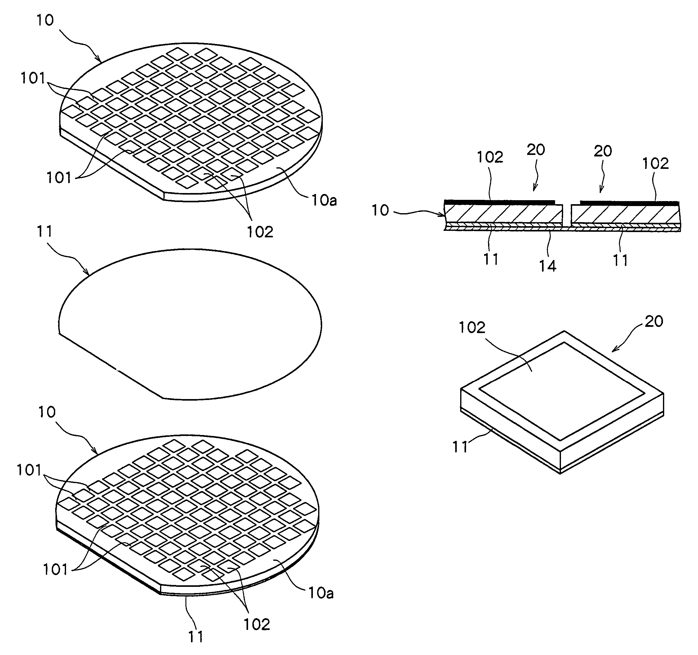
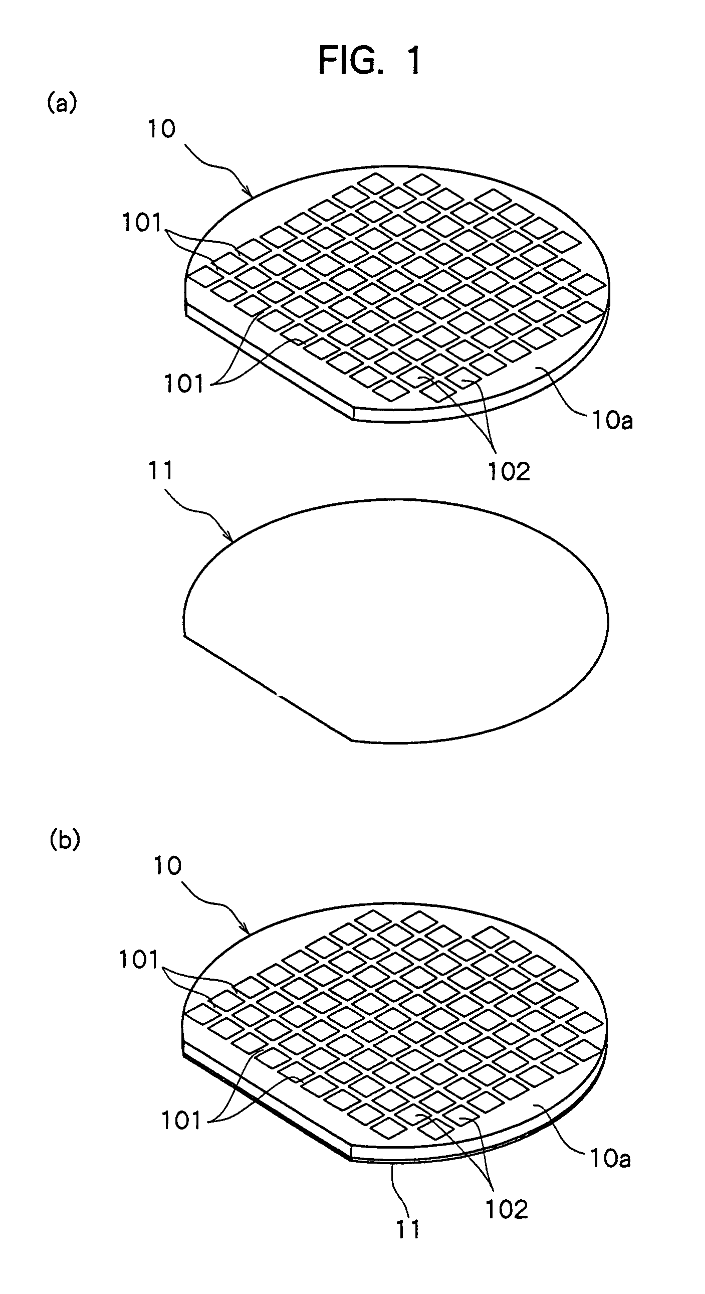
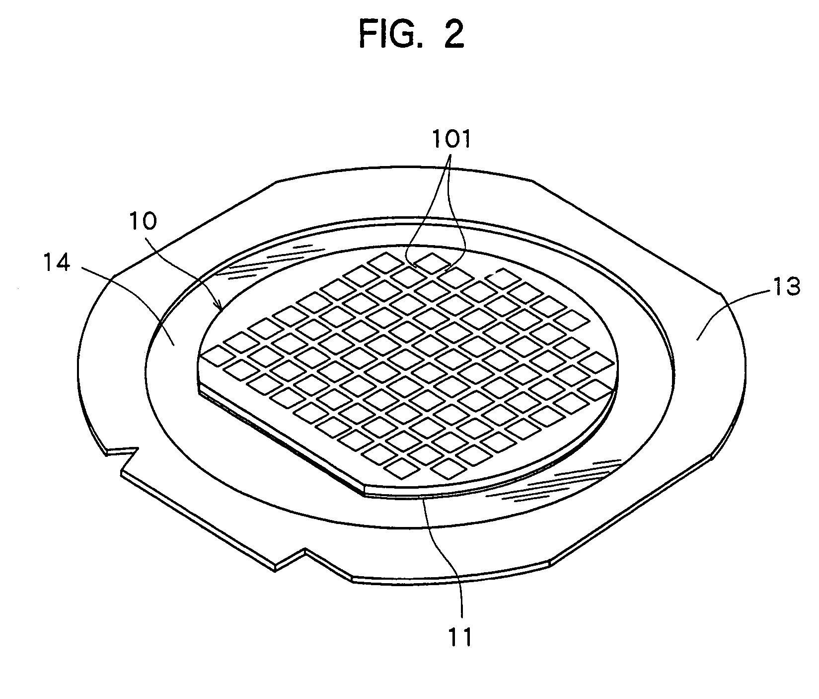
[0027]FIGS. 1(a) and 1(b) are diagrams showing an example of the bonding film adhering step of adhering a bonding film for die bonding to the back surface of a semiconductor wafer in the dividing method of the present invention.

[0028]FIG. 1(a) is a perspective view of a semiconductor wafer 10 and a bonding film 11 for die bonding to be adhered to the back surface of the semiconductor wafer 10. A plurality of streets 101 are formed on the front surface 10a of the semiconductor wafer 10 in a lattice form, and a circuit 102 is formed in a plurality of areas sectioned by the plurality of streets 101. A film material that is made from a polyimide resin and has a thickness of 20 to 40 μm may be used as the bonding film 11 for die bonding. This bonding film 11 for die bonding is placed on the back surface of ...


PUM

PropertyMeasurementUnit
temperatureaaaaaaaaaa
thicknessaaaaaaaaaa
thicknessaaaaaaaaaa

Abstract

A method of dividing a semiconductor wafer comprising:a bonding film adhering step of adhering a bonding film for die bonding to the back surface of the semiconductor wafer;a protective adhesive tape affixing step of affixing an extensible protective adhesive tape to the bonding film side of the semiconductor wafer having the bonding film on the back surface;a dividing step of dividing the semiconductor wafer affixed to the protective adhesive tape into individual semiconductor chips by applying a laser beam along the streets;a bonding film breaking step of breaking the bonding film for every semiconductor chip by extending the protective adhesive tape so as to give tensile force to the bonding film; anda semiconductor chip removing step of removing the semiconductor chips having the broken bonding film from the protective adhesive tape.

Description

FIELD OF THE INVENTION[0001]The present invention relates to a method of dividing a semiconductor wafer having a plurality of streets formed on the front surface in a lattice form and a circuit formed in a plurality of areas sectioned by the plurality of streets into individual semiconductor chips.DESCRIPTION OF THE PRIOR ART[0002]In the production process of semiconductor devices, for example, semiconductor chips are manufactured by forming a circuit such as IC, LSI or the like in a large number of areas sectioned by streets (cutting lines) formed on the front surface of a substantially disk-like semiconductor wafer in a lattice form and by dividing the areas having the circuit formed therein along the streets. A dicing machine is generally used as the dividing machine for dividing a semiconductor wafer, and the dicing machine cuts a semiconductor wafer with a cutting blade having a thickness of about 20 μm. These semiconductor chips are packaged, and widely used in electric applia...

Claims


Application Information

Patent Timeline
Patent Type & Authority Patents(United States)
IPC IPC(8): H01L21/78B26D3/00B23K26/40B28D5/00H01L21/00H01L21/301H01L21/68
CPCB23K26/0057B23K26/4075B28D5/0011B28D5/0052H01L21/6835H01L21/6836H01L21/78H01L21/67132H01L2221/68327H01L2221/68336B23K26/40B23K26/53B23K2103/50Y10T83/02E02D13/04E02D5/30E02D5/526E02D17/04E02D2300/006
Inventor KAWAI, AKIHITO
Owner DISCO CORP
Why Eureka
Try Eureka