Integrated circuit including an overvoltage protection circuit

a protection circuit and integrated circuit technology, applied in the direction of logic circuit coupling/interface arrangement, pulse technique, instruments, etc., can solve the problems of deterioration or destruction of the output mos transistor, higher cost, and a larger mounting surface, so as to withstand voltage can be set low, and reduce the circuit area of the output transistor and the chip area

Inactive Publication Date: 2006-10-31
RENESAS ELECTRONICS CORP
View PDF6 Cites 74 Cited by
  • Summary
  • Abstract
  • Description
  • Claims
  • Application Information

AI Technical Summary

Benefits of technology

[0025]According to one aspect of the invention, there is provided an integrated circuit which includes an output transistor connected between a power supply and an inductive load, and controlling a current flowing into the inductive load; a clamp circuit clamping an overvoltage applied to the output transistor; and a clamp control circuit activating the clamp circuit upon detection of a back electromotive force (EMF) by the inductive load. In this integrated circuit, the clamp circuit operates only when a back EMF occurs, such as in a turn-off period. This allows a withstand voltage of the output transistor to be set without consideration of a withstand voltage of the clamp circuit and so on; thus, the withstand voltage can be set low. It is thereby possible to reduce a circuit area of the output transistor and a chip area.
[0026]According to another aspect of the invention, there is provided an integrated circuit which includes an output transistor having a drain connected to a power supply and a source connected to an inductive load; a first transistor and a dynamic clamp circuit connected in series between the power supply and a gate of the output transistor; and a second transistor connected between the power supply and the inductive load, and turning on or off the first transistor according to a change in a gate voltage of the output transistor. In this integrated circuit, the dynamic clamp circuit operates only when a back EMF occurs, such as in a turn-off period. This allows a withstand voltage of the output transistor to be set without consideration of a withstand voltage of the dynamic clamp circuit and so on; thus, the withstand voltage can be set low. It is thereby possible to reduce a circuit area of the output transistor and a chip area.
[0027]According to yet another aspect of the invention, there is provided an integrated circuit which includes a high side switching device driving an inductive load; a control voltage generation circuit generating a control voltage which controls an operation of the high side switching device; and a back electromotive force (EMF) protection circuit protecting the high side switching device from a back electromotive force when the control voltage changes. In this integrated circuit, the back EMF protection circuit operates only when a back EMF occurs, such as in a turn-off period. This allows a withstand voltage of the high side switching device to be set without consideration of a withstand voltage of the back EMF protection circuit and so on; thus, the withstand voltage can be set low. It is thereby possible to reduce a circuit area of the high side switching device and a chip area.
[0028]The present invention can prevent an increase in a chip area, reduce costs, and avoid an increase in a mounting area, even with the dynamic clamp circuit.

Problems solved by technology

This can cause characteristics degradation or destruction of the output MOS transistor M10.
The increase in the chip area causes higher costs and a larger mounting surface.

Method used


Image

  • Integrated circuit including an overvoltage protection circuit
  • Integrated circuit including an overvoltage protection circuit
  • Integrated circuit including an overvoltage protection circuit

Examples


first embodiment

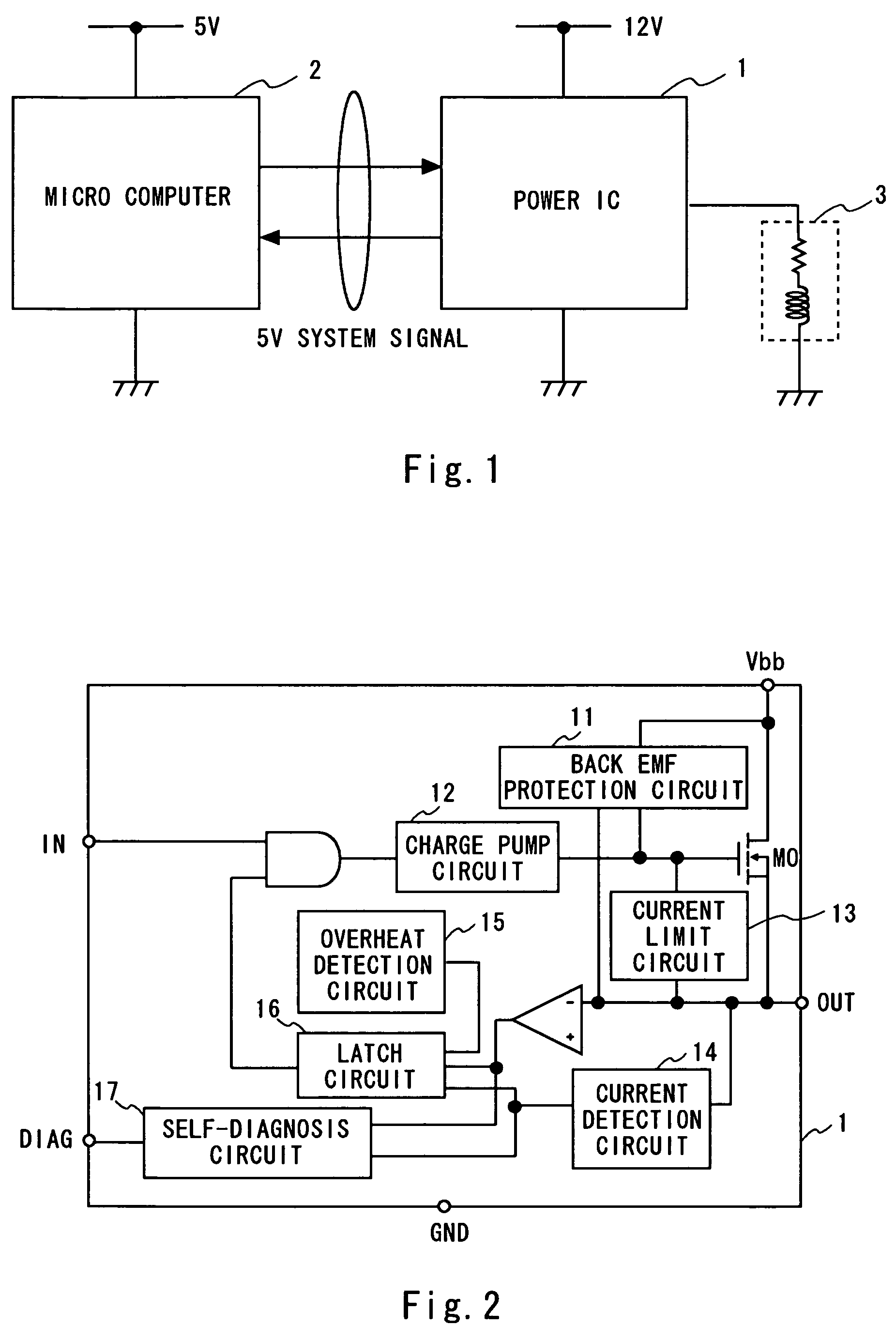
[0043]Referring first to FIG. 1, the configuration of a system having a power IC according to a first embodiment of the invention is explained. The system controls the current flowing into an L load. It includes a power IC 1, a microcomputer 2, and an L load 3. Though the power IC 1 and the microcomputer 2 are each an integrated circuit on one chip in this example, they may be implemented on a given number of chips.

[0044]The microcomputer 2 is connected to the power IC 1 to exchange signals. The microcomputer 2 transmits to the power IC 1 a control signal which controls the current of the L load 3 and receives from the power IC 1 a diagnostic signal which indicates the state of the power IC 1 and so on. The microcomputer 2 is, for example, driven by a power source of 5V, and the signal transmitting to or receiving from the power IC 1 has an amplitude of 5V.

[0045]The power IC 1 is connected to the microcomputer 2 and to the L load 3. The power IC 1 controls the current flowing into t...

second embodiment

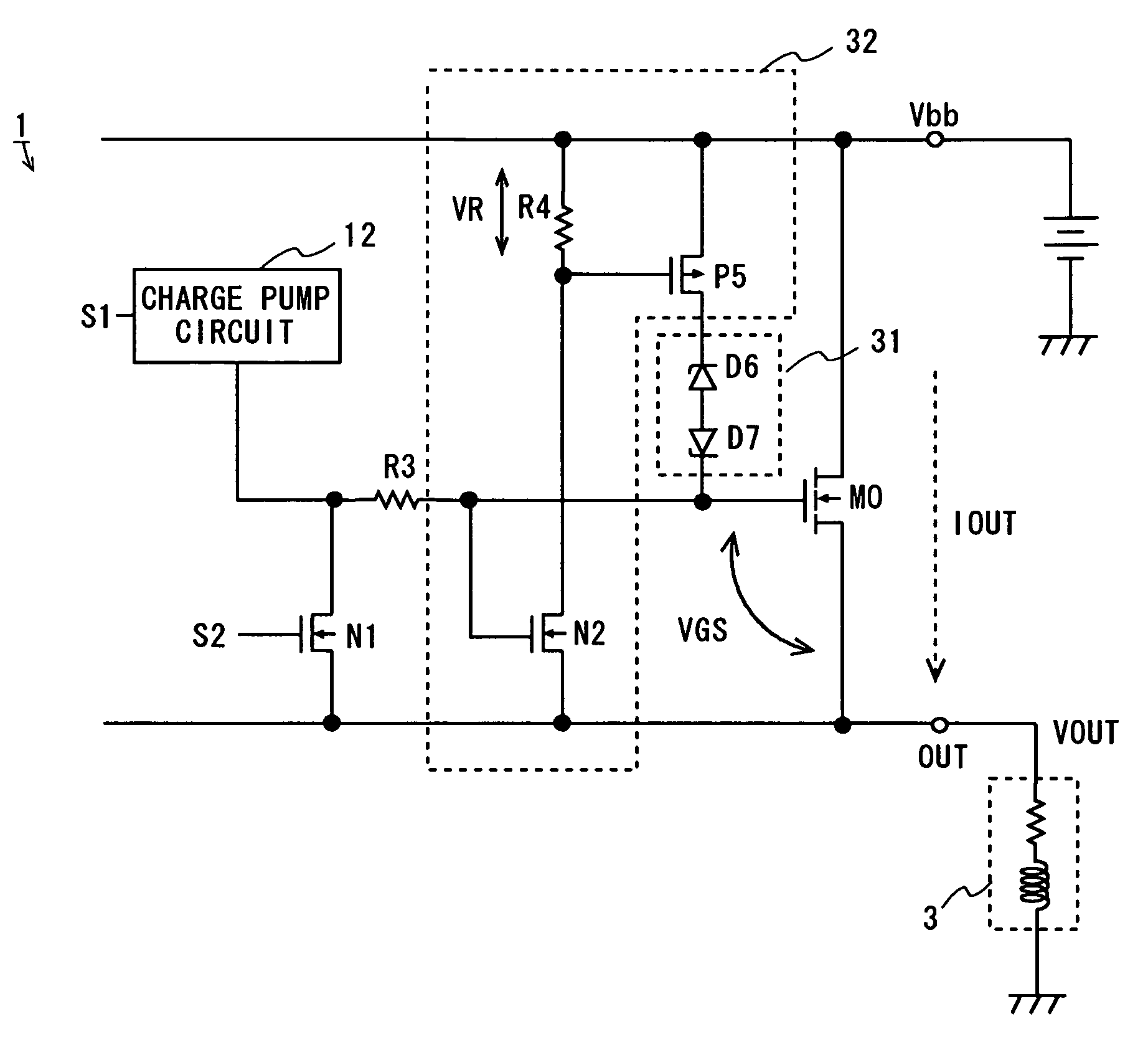
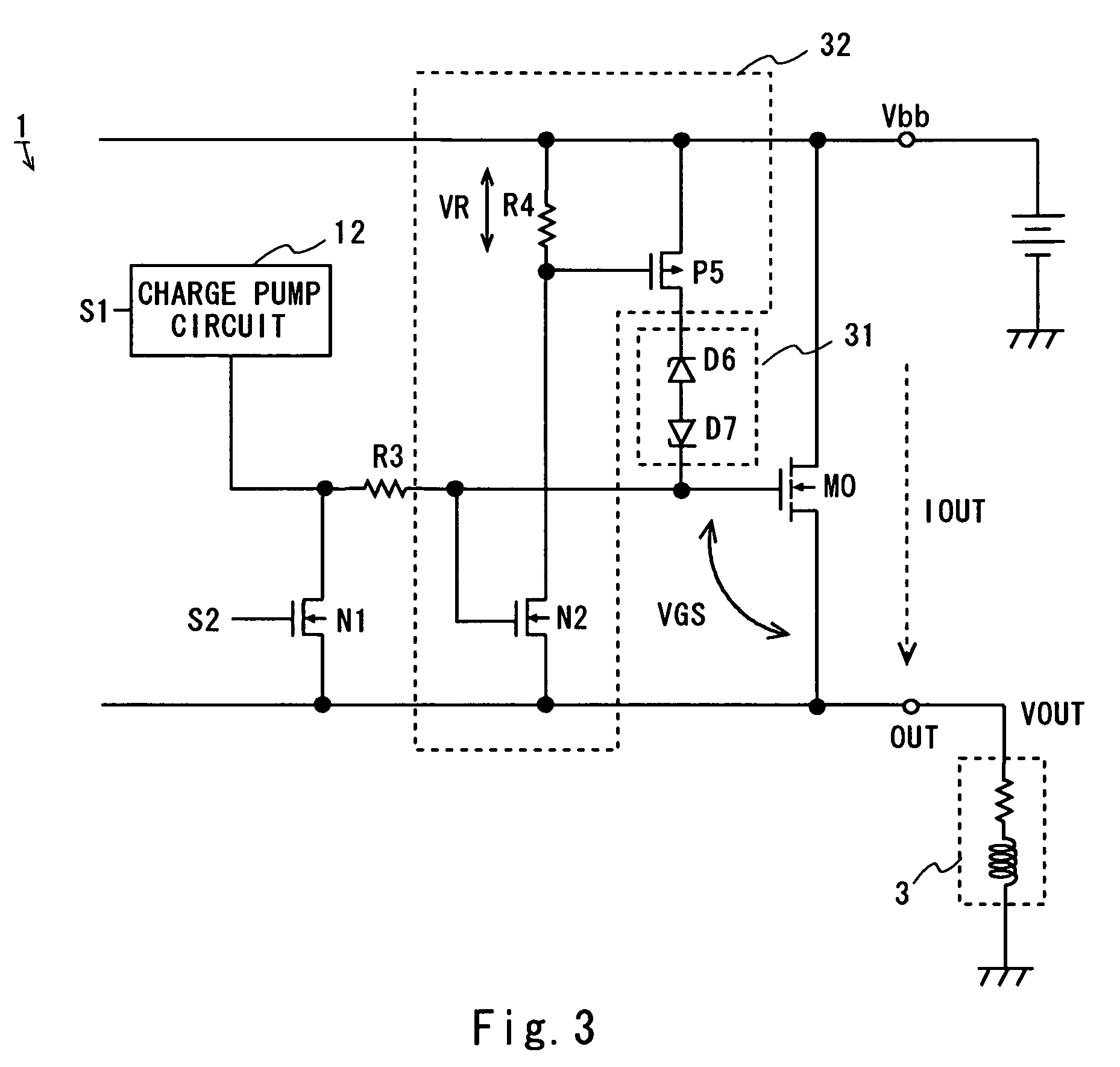
[0078]Referring now to FIG. 6, the circuit configuration of a power IC of a second embodiment is explained. Like FIG. 3, FIG. 6 illustrates the part of the circuit including the output MOS transistor M0, the back EMF protection circuit 11, and the charge pump circuit 12 of the power IC 1 of FIG. 2.

[0079]The power IC 1 of this embodiment has a resistor R3′ between the resistor R3 and the gate of the output MOS transistor MO in addition to the elements shown in FIG. 3. The gate of the gate detection MOS transistor N2 is connected to a node between the resistor R3 and the resistor R3′.

[0080]In this embodiment, the gate detection MOS transistor N2 refers to the gate voltage of the output MOS transistor M0 which drops across the resistor R3′. This configuration also allows the same operation as the configuration of FIG. 3.

third embodiment

[0081]Referring then to FIG. 7, the circuit configuration of a power IC of a third embodiment is explained. Like FIG. 3, FIG. 7 illustrates the part of the circuit including the output MOS transistor M0, the back EMF protection circuit 11, and the charge pump circuit 12 of the power IC 1 of FIG. 2.

[0082]The power IC 1 of this embodiment has a constant current source I1 and a diode D8 between the Vbb terminal and the gate of the output MOS transistor M0 in addition to the elements shown in FIG. 3. The gate of the gate detection MOS transistor N2 is connected to a node between the constant current source I1 and the diode D8.

[0083]In this embodiment, the gate detection MOS transistor N2 refers to the gate voltage of the output MOS transistor M0 which is boosted by the diode D8. This configuration also allows the same operation as the configuration of FIG. 3.


PUM


Abstract

The power IC includes an output transistor M0 which controls a current flowing into an L load, a dynamic clamp circuit which clamps an overvoltage, and a clamp control circuit which controls the operation of the dynamic clamp circuit. The clamp control circuit activates the dynamic clamp circuit, which is normally inactive, upon detection of a back EMF by the L load.

Description

BACKGROUND OF THE INVENTION[0001]1. Field of the Invention[0002]The present invention relates to integrated circuits and, particularly, to an integrated circuit including an overvoltage protection circuit for an output MOS transistor.[0003]2. Description of Related Art[0004]A power integrated circuit (IC), which is also called a power semiconductor, is used in vehicles and home electric appliances to control a voltage and current. Miniaturization of the power IC is required.[0005]For example, a vehicle has an actuator that converts an electrical signal into mechanical motion for fuel control or transmission control. A power IC is used to control on / off of the current flowing into the actuator.[0006]FIG. 9 shows a normal vehicle electric system. An example is described in “CAR ELECTRONICS AND RELIABILITY ENHANCEMENT OF IN-VEHICLE ELECTRONIC PARTS AND DEVICES”, first edition, Technical Institution Institute Co. Ltd, Jul. 31, 1989, p. 31 (FIG. 2). The vehicle electric system includes a...

Claims


Application Information

Patent Timeline
Patent Type & Authority Patents(United States)
IPC IPC(8): H03K3/00H01L27/04H01L21/822H03K17/06H03K17/08H03K17/082H03K17/695H03K19/0175
CPCH03K17/063H03K17/0822H03K2017/0806
Inventor FUKAMI, IKUO
Owner RENESAS ELECTRONICS CORP
Why Eureka
Try Eureka