Method and apparatus for testing image sensors

a technology of image sensor and test method, which is applied in the direction of instruments, material analysis, television systems, etc., can solve the problems of inaccurate test method, inability to perform the proper function, and inability to accurately test image sensor,

Active Publication Date: 2006-11-14
APTINA IMAGING CORP
View PDF13 Cites 28 Cited by
  • Summary
  • Abstract
  • Description
  • Claims
  • Application Information

AI Technical Summary

Benefits of technology

[0019]The present invention is particularly useful for testing a wide variety of image sensor failing mechanisms and for automating the image sensor testing process.

Problems solved by technology

Image sensor pixel arrays, such as the CMOS imager described above, are subject to various failing mechanisms, which ultimately result in a defective imagers.
For example, pixel arrays can be short circuited or open circuited during fabrication and therefore may not perform their proper function.
The accuracy of this method of testing image sensors, however, is a concern.
Defect detection is especially difficult when it is dependent on human observation of the output as displayed on the viewing device (e.g. a cathode ray tube or liquid crystal display panel).
As the number of pixels on an integrated circuit expands, it becomes increasingly difficult for a human to detect faults.
Unfortunately, humans lack consistent observational skills due to their very nature and varying levels of alertness throughout the day.
Therefore, this type of testing is not acceptable for high volume, cost sensitive, image sensor products.
Other image sensor testing techniques have problems as well.
This alignment process can be difficult and time consuming.
Furthermore, static test images are not capable of testing an image sensor for various failing mechanisms across the entire pixel array.

Method used


Image

  • Method and apparatus for testing image sensors
  • Method and apparatus for testing image sensors
  • Method and apparatus for testing image sensors

Examples


Embodiment Construction

[0030]In the following detailed description, reference is made to the accompanying drawings which form a part hereof, and in which is shown by way of illustration specific embodiments in which the invention may be practiced. These embodiments are described in sufficient detail to enable those of ordinary skill in the art to make and use the invention, and it is to be understood that structural, logical or procedural changes may be made to the specific embodiments disclosed without departing from the spirit and scope of the present invention.

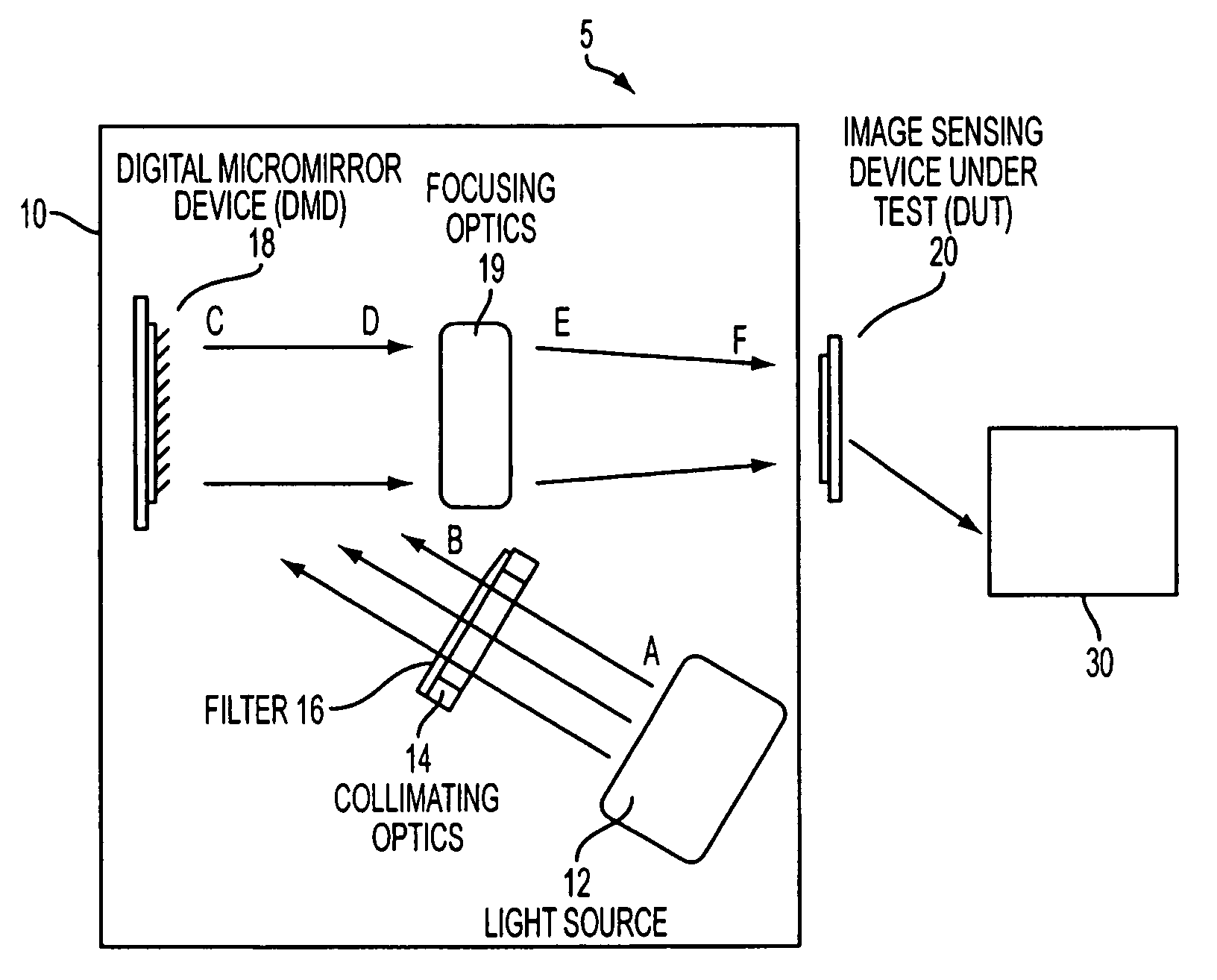
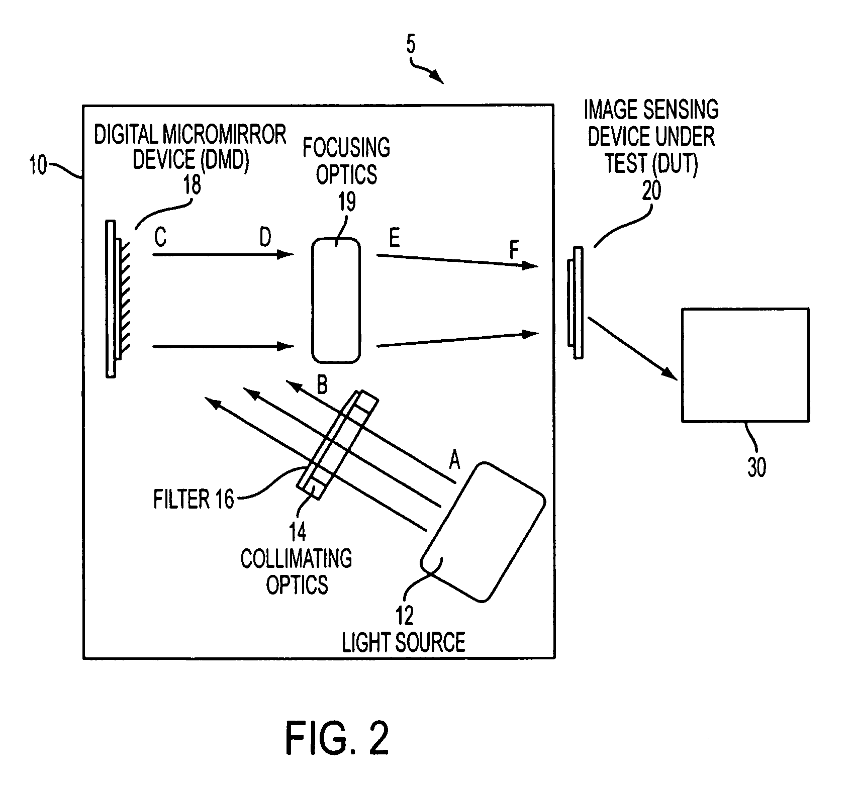
[0031]FIG. 2 is a representation of the image sensor testing apparatus according to a first exemplary embodiment of the present invention. The apparatus 5 comprises a digital light processing system (DLPS) 10 capable of projecting high-resolution images onto an image sensing device under test (DUT) 20, such as the CMOS imager described above, and an image sensor signal detector 30 capable of reading the output of the DUT 20. The DLPS 10 is capabl...


PUM

PropertyMeasurementUnit
digital light processing controlaaaaaaaaaa
charge levelaaaaaaaaaa
transfer of chargeaaaaaaaaaa

Abstract

Methods and apparatuses for testing image sensors are disclosed. Desirable apparatuses of the present invention include image sensor testing devices comprising a digital light projection system capable of projecting static or dynamic images onto an image sensing device under test and an image sensor signal detection means for analyzing the output of said image sensing device under test. The digital light projection system comprises a light source, collimating optics, a digital micromirror device, and focusing optics. Other desirable methods and apparatuses of the present invention include image sensor testing devices employing a digital light projection system capable of simultaneously testing a plurality of image sensors. According to the present invention, the light source is calibrated and converted to a desired test image by the digital micromirror device. The test image is then focused onto an image sensor, the output of which is read by a detector and correlated with the input digital test image.

Description

FIELD OF THE INVENTION[0001]This invention relates generally to a method and apparatus for testing image sensors and, more particularly, to a method and apparatus for the automated testing of a single image sensor or a plurality of image sensors using both static and dynamic test patterns.BACKGROUND OF THE INVENTION[0002]A conventional image sensor is composed of an array of individual light sensitive circuits called pixels that are organized in rows and columns. A row of pixels has a common line connecting the control gates of their respective access transistors. Data is passed from a pixel through its access transistor to a data line. Each column of pixels is connected to a common data line.[0003]There are a number of different types of semiconductor-based imagers including charge coupled devices (CCD), photodiode arrays, and complementary metal-oxide semiconductor (CMOS) imagers. A CMOS imager circuit, for example, includes a focal plane array of pixel cells; each cell includes a...

Claims


Application Information

Patent Timeline
Patent Type & Authority Patents(United States)
IPC IPC(8): G01N21/00H04N5/374H04N17/00
CPCH04N17/002H04N17/00
Inventor GOMM, TYLER J.BRUCE, JEFF D.
Owner APTINA IMAGING CORP
Why Eureka
Try Eureka