Timing adjustment circuit and semiconductor device including the same

Inactive Publication Date: 2006-11-14
LONGITUDE SEMICON S A R L
View PDF7 Cites 24 Cited by
  • Summary
  • Abstract
  • Description
  • Claims
  • Application Information

AI Technical Summary

Benefits of technology

[0025]According to the present invention, the phase advance/delay signal generation circuit is disposed in the timing adjustment circuit. Accordingly, it is possible to provide the semicond

Problems solved by technology

In semiconductor devices such as a synchronous memory which operates in synchronization with an external clock signal (clock synchronous type semiconductor memories such as SDRAM) and a controller (a system LSI or microprocessor), with speeding-up of the operation, a propagation delay of a clock signal in an apparatus has raised a problem.
Accordingly, there has been a problem that a phase difference between the external clock signal and the internal clock signal deviates from a predetermined value (timing deviation).
Specifically, with enhanc

Method used


Image

  • Timing adjustment circuit and semiconductor device including the same
  • Timing adjustment circuit and semiconductor device including the same
  • Timing adjustment circuit and semiconductor device including the same

Examples


first embodiment

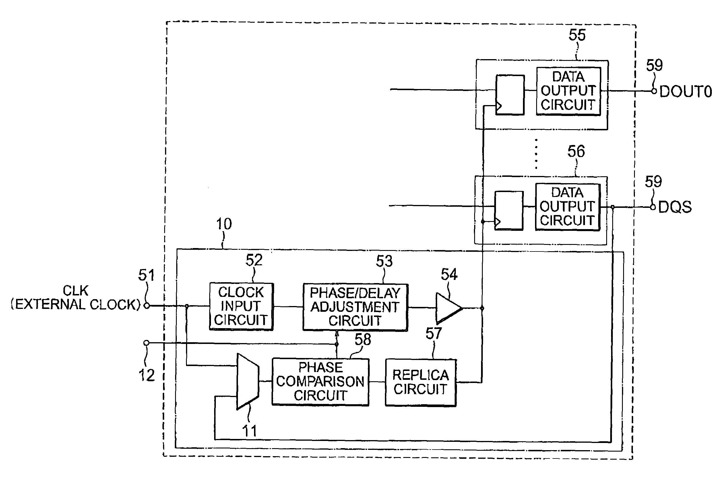
[0033]FIG. 3 shows a block diagram of a timing adjustment circuit according to the present invention. In addition to a constitution of a timing adjustment circuit 50 of FIG. 1, a timing adjustment circuit 10 includes a selector 11, and an external output terminal 12 for extracting an output of a phase comparison circuit 58 to the outside.

[0034]The selector 11 includes two input terminals, one of the input terminals is connected to an external clock input terminal 51, and the other is connected to an output terminal 59 of a data strobe output circuit 56. The output terminal of the selector 11 is connected to one input terminal of the phase comparison circuit 58. The selector 11 selectively outputs either one of an inputted external clock signal CLK and data strobe signal DQS to the phase comparison circuit 58.

[0035]Next, a method of removing (reducing) a timing deviation of the timing adjustment circuit of FIG. 3 will be described. When the timing deviation is removed, the selector 1...

second embodiment

[0050]Subsequently, description will be made of the present invention with reference to FIG. 5.

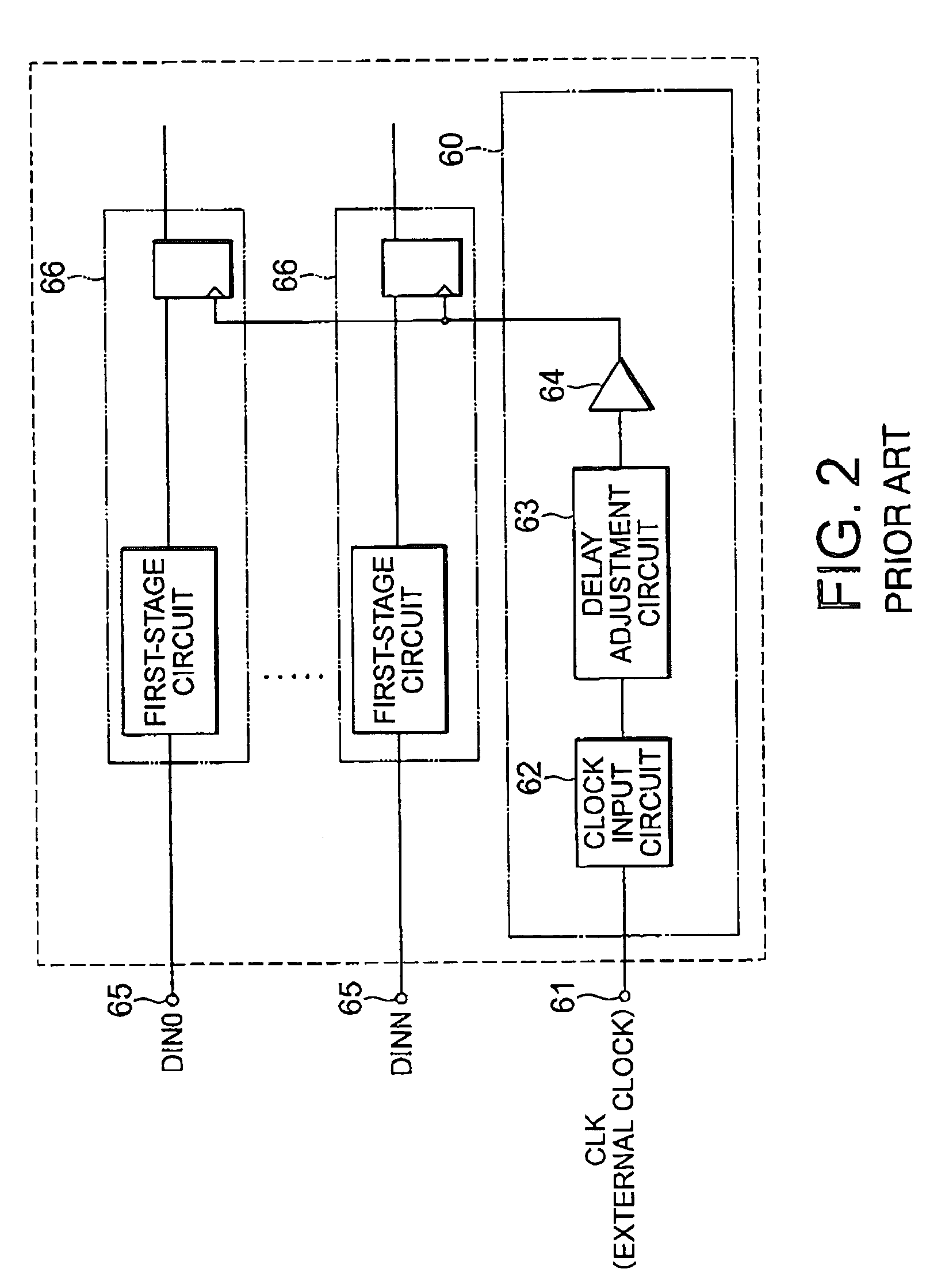
[0051]In addition to the constitution of FIG. 2, a timing adjustment circuit 30 illustrated in FIG. 5 includes a replica circuit 31 including the same constitution as that of a data input circuit 66.

[0052]The replica circuit 31 includes an initial-stage circuit 32 and latch circuit 33, and is connected between an external clock input terminal 61 and an external output terminal 34. The latch circuit 33 is connected to a clock driver 64.

[0053]When a external clock signal CLK is inputted into the external clock input terminal 61 of the timing adjustment circuit 30 illustrated in FIG. 5, the external clock signal CLK is given to a clock input circuit 62 and replica circuit 31.

[0054]Upon receiving the external clock signal CLK, the clock input circuit 62 outputs the signal as the input clock signal to a delay adjustment circuit 63. The delay adjustment circuit 63 delays the external clock signa...


PUM


Abstract

In order to compare a phase of an internal clock signal outputted from a clock driver with that of a data strobe signal from a data strobe output circuit driven by the internal clock signal, a selector is disposed to supply a data strobe signal instead of an external clock signal inputted into a phase comparison circuit. While the selector selects the data strobe signal, the selector, a replica circuit, and the phase comparison circuit operate as a phase advance/delay signal generation circuit to output a phase advance/delay signal indicating a timing deviation to an external output terminal.

Description

[0001]This application claims priority to prior application JP 2002-311231, the disclosure of which is incorporated herein by reference.BACKGROUND OF THE INVENTION[0002]The present invention relates to a timing adjustment circuit for producing an internal clock signal which has a predetermined phase relation with respect to an inputted external clock signal and to a semiconductor device including the timing adjustment circuit.[0003]In semiconductor devices such as a synchronous memory which operates in synchronization with an external clock signal (clock synchronous type semiconductor memories such as SDRAM) and a controller (a system LSI or microprocessor), with speeding-up of the operation, a propagation delay of a clock signal in an apparatus has raised a problem. To solve the problem, in the conventional semiconductor device, a timing adjustment circuit is disposed in an interface (or an input / output device) to receive an external clock signal and to produce an internal clock wh...

Claims


Application Information

Patent Timeline
IPC IPC(8): G06F1/12G01R31/28G06F1/06G06F1/10G11C7/10G11C11/407H03K5/00H03K5/135H03L7/06H03L7/081
CPCG11C7/1051G11C7/106G11C7/1066G11C7/222H03L7/0812H03L7/0816
Inventor ISHIKAWA, TORU
Owner LONGITUDE SEMICON S A R L
Why Eureka
Try Eureka