Energy recovering circuit with boosting voltage-up and energy efficient method using the same

a technology of energy recovery circuit and power supply, which is applied in the direction of dc-dc conversion, power conversion systems, instruments, etc., can solve the problems of increasing energy loss, and reducing the energy recovery efficiency of the panel. , to achieve the effect of improving the energy recovery efficiency and reducing the charging time of the panel

Inactive Publication Date: 2006-11-21
LG ELECTRONICS INC
View PDF39 Cites 29 Cited by
  • Summary
  • Abstract
  • Description
  • Claims
  • Application Information

AI Technical Summary

Benefits of technology

[0017]Accordingly, it is an object of the present invention to provide an energy recovering circuit and an energy efficient

Problems solved by technology

Generally, a plasma display panel (PDP) has a disadvantage of large power consumption.
When such a charge/discharge is generated at the PDP, a capacitive load of the panel does not cause an energy waste, but a lot of energy loss occurs at the PDP because a direct current (DC) power source is used to generate a driving pulse.
Particularly, if an excessive current flows in the cell upon discharge, then an energy loss is increased.
This energy loss causes a temperature rise of switching devices, which may break the switching devices in the worst case.
However, because the conventional energy recovering circuit as in FIG. 1 uses the same inductor L on the charge/discharge path, if the rising time is made to be fast by

Method used


Image

  • Energy recovering circuit with boosting voltage-up and energy efficient method using the same
  • Energy recovering circuit with boosting voltage-up and energy efficient method using the same
  • Energy recovering circuit with boosting voltage-up and energy efficient method using the same

Examples


first embodiment

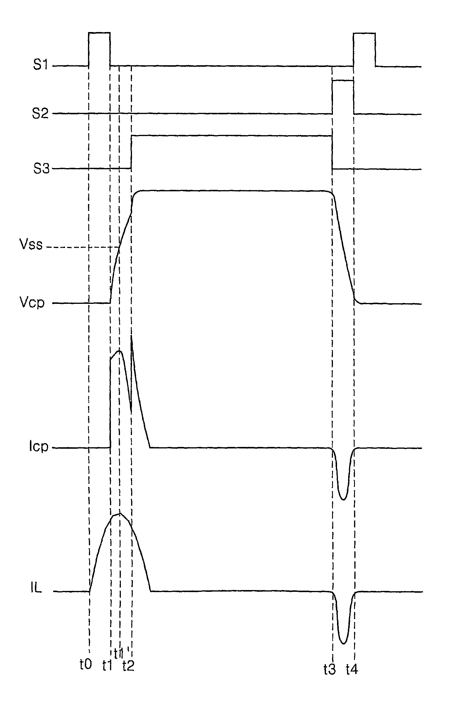
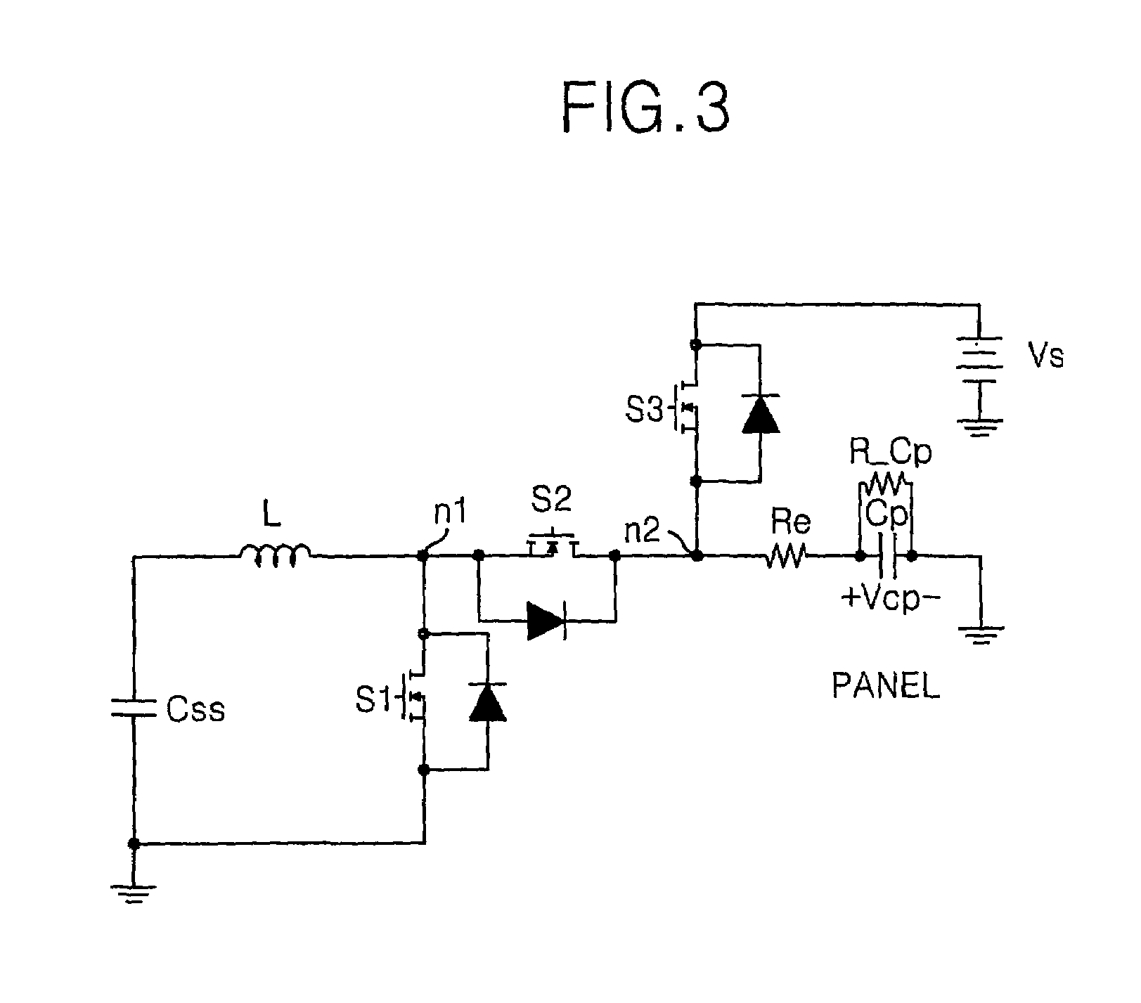
[0087]Referring to FIG. 3, an energy recovering circuit according to the present invention includes an capacitor Css, an inductor L and a first switch S1 connected to form a closed loop; a second switch S2 connected, via a second node n2, to a panel capacitor Cp; and a third switch S3 connected between a second node n2 and a sustaining voltage source vs.

[0088]The panel capacitor Cp represents a capacitance value of the panel, and reference numerals Re and R-Cp represent parasitic resistances of an electrode and a cell provided at the panel, respectively. Each of the switches S1, S2 and S3 is implemented by a semiconductor switching device, for example, MOS FET, IGBT, SCR, BJT and etc.

[0089]While the first switch S1 is turned on, there is formed a closed loop of electric current which starts from the terminal of one side of the capacitor Css and is connected to the terminal of another side of the capacitor Css, via the inductor L and the first switch S1. Electric current is accumulat...

second embodiment

[0104]Referring to FIG. 8, there is shown an energy recovering circuit according to the present invention.

[0105]Referring to FIG. 8, an energy recovering circuit according to a second embodiment of the present invention includes an capacitor Css, an inductor L, a first switch S1 and a fourth switch S4 connected to form a closed loop; a second switch S2 commonly connected, via a first node n1, to the first and the fourth switches S1 and S4 and connected, via a second node n2, to a panel capacitor Cp; and a third switch S3 connected between a second node n2 and a sustaining voltage source vs.

[0106]Each of the switches S1, S2 and S3 is implemented by a semiconductor switching device, for example, MOS FET, IGBT, SCR, BJT and etc.

[0107]When the first switch S1 and the fourth switch S4 are turned on, there is formed a closed loop of electric current which starts from the terminal of one side of the capacitor Css and is connected to the terminal of another side of the capacitor Css, via th...

third embodiment

[0117]FIG. 11 shows an energy recovering circuit according to the present invention.

[0118]Referring to FIG. 11, an energy recovering circuit according to a third embodiment of the present invention includes an capacitor Css, an inductor L and a first switch S1 connected to form a closed loop; a bridge circuit 10 commonly connected, via a first node n1, to the inductor L and the first switch S1 and connected, via a second node n2, to a panel capacitor Cp; a third switch S3 connected between a second node n2 and a sustaining voltage source vs; and a fourth switch S4 connected between the second node n2 and a ground voltage source GND.

[0119]The bridge circuit 10 consists of diodes Dc1, Dc2, Dr1 and Dr2 connected in a bridge type between the first node n1 and the second node n2, and a second switch S2 connected to the diodes Dc1, Dc2, Dr1 and Dr2. The bridge circuit 10 controls a current path upon the charge / discharge time of the panel.

[0120]Each of the switches S1, S2 and S3 is impleme...


PUM


Abstract

There is disclosed an energy recovering circuit with boosting voltage-up and an energy efficient method using the same that are capable of boosting the voltage factor of an energy recovered from the panel to rapidly re-appl it to the panel, to thereby reduce the charging time of a panel capacitor and improve its energy recovery efficiency. An energy recovering circuit according to the present invention includes a voltage boosting circuit for boosting a voltage factor of an energy recovered from a panel and supplying the boosted energy to the panel. An energy efficient method according to the present invention includes steps of recovering an energy from a panel to a closed loop; and a controlling the closed loop in order to supplying the energy with its voltage factor boosted to the panel.

Description

TECHNICAL FIELD[0001]This invention relates to an energy recovering apparatus for a plasma display panel, and more particularly to an energy recovering circuit with boosting voltage-up and an energy efficient method using the same that are capable of boosting the voltage factor of an energy recovered from the panel to rapidly re-apply it to the panel, to thereby reduce the charging time of a panel capacitor and improve its energy recovery efficiency.[0002]Also, this invention relates to an energy recovering circuit and an energy efficient method using the same that are capable of reducing the number of necessary devices.BACKGROUND ART[0003]Generally, a plasma display panel (PDP) has a disadvantage of large power consumption. A reduction of such power consumption requires enhancing a light-emitting efficiency and minimizing an unnecessary energy waste occurring in a driving process without a direct relation to a discharge.[0004]An alternating current (AC)-type PDP coats an electrode ...

Claims


Application Information

Patent Timeline
IPC IPC(8): G09G3/28G09G5/00G09G3/20G09G3/288H02M3/155
CPCG09G3/2965G09G2310/06G09G3/296
Inventor CHO, JANG-HWANLEE, NAM-KYUKIM, CHEUL-UKANG, FEEL-SOONLEE, EUNG-KWANRYU, JAE-HWAKANG, SUNG-HO
Owner LG ELECTRONICS INC
Why Eureka
Try Eureka